

Method of forming a ferroelectric device
a technology of ferroelectric devices and ferroelectric patterns, which is applied in the direction of semiconductor devices, electrical devices, capacitors, etc., can solve the problems of small loss of ferroelectric patterns and small defects generated by cmp processes, and achieve the effect of low polishing ra
- Summary
- Abstract
- Description
- Claims
- Application Information
AI Technical Summary
Benefits of technology
Problems solved by technology
Method used
Image

Examples
first embodiment
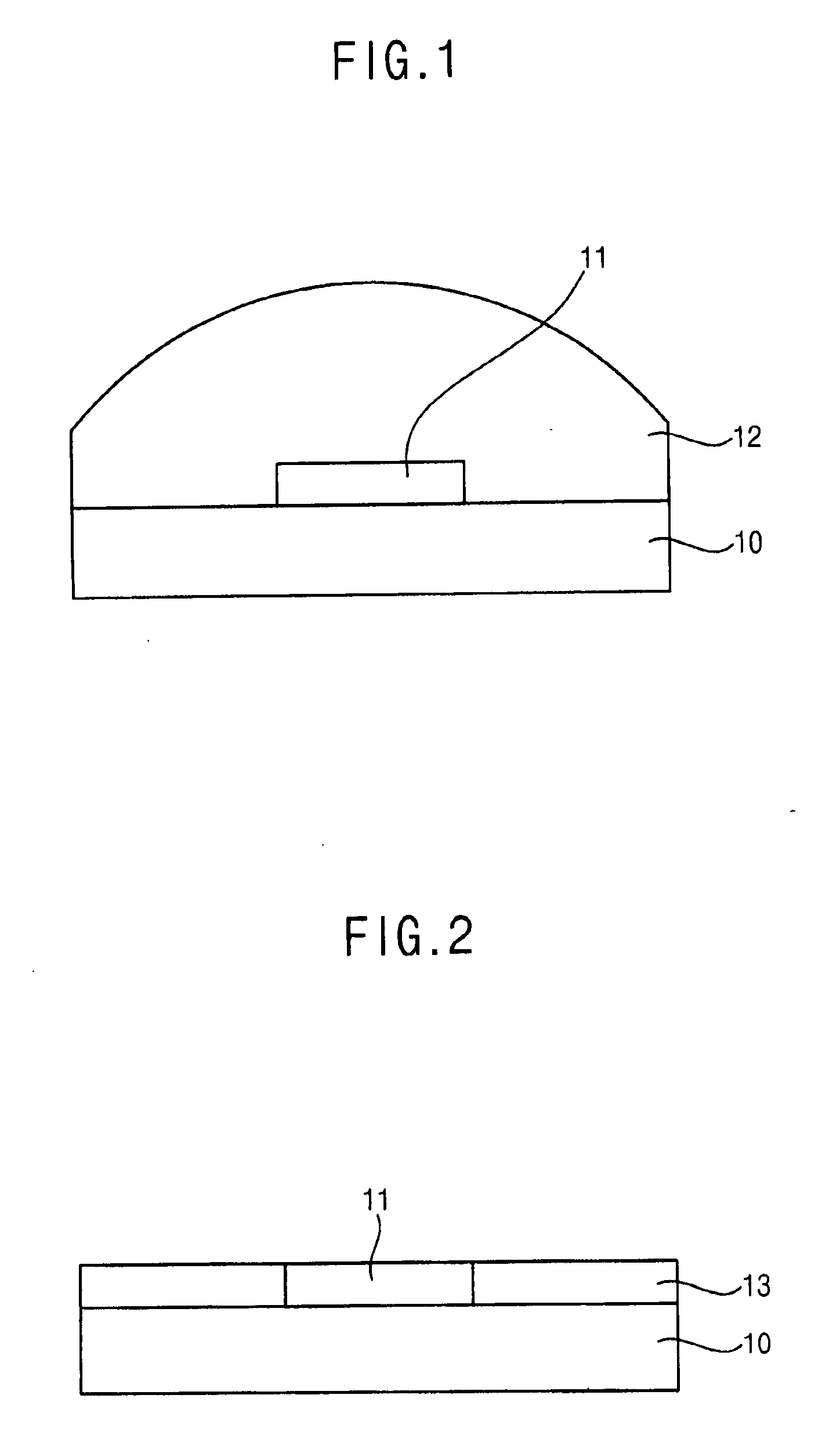
[0039]FIGS. 1-2 illustrate cross-sectional views of stages in a chemical mechanical polishing method in accordance with the present invention. Referring to FIG. 1, a ferroelectric pattern 11 may be provided on a lower structure 10. The lower structure 10 may be, e.g., a substrate, and may include one or more layers. The ferroelectric pattern 11 may include a ferroelectric material including titanium and oxygen, e.g., one or more of PZT [Pb Zr, Ti O3], SBT [SrBi2Ti2O9], BLT [Bi La, Ti O3], PLZT [Pb La, Zr TiO3], BST [Bi Sr, Ti O3], etc.
[0040]An insulating layer 12 may be formed on the lower structure 10 and may cover the ferroelectric pattern 11. The insulating layer 12 may include, e.g., oxide, nitride, oxynitride, etc. For example, the insulating layer 12 may include one or more of boro-phosphor silicate glass (BPSG), phosphor silicate glass (PSG), undoped silicate glass (USG), spin-on-glass (SOG), flowable oxide (FOX), plasma-enhanced tetra-ethyl-ortho-silicate (PE-TEOS), high den...
second embodiment
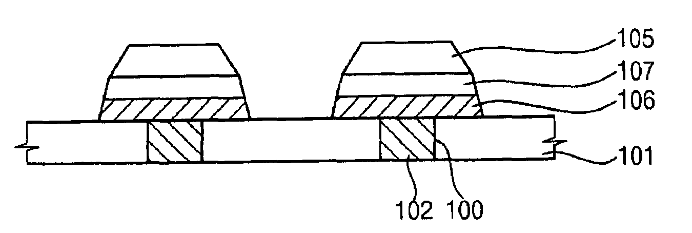
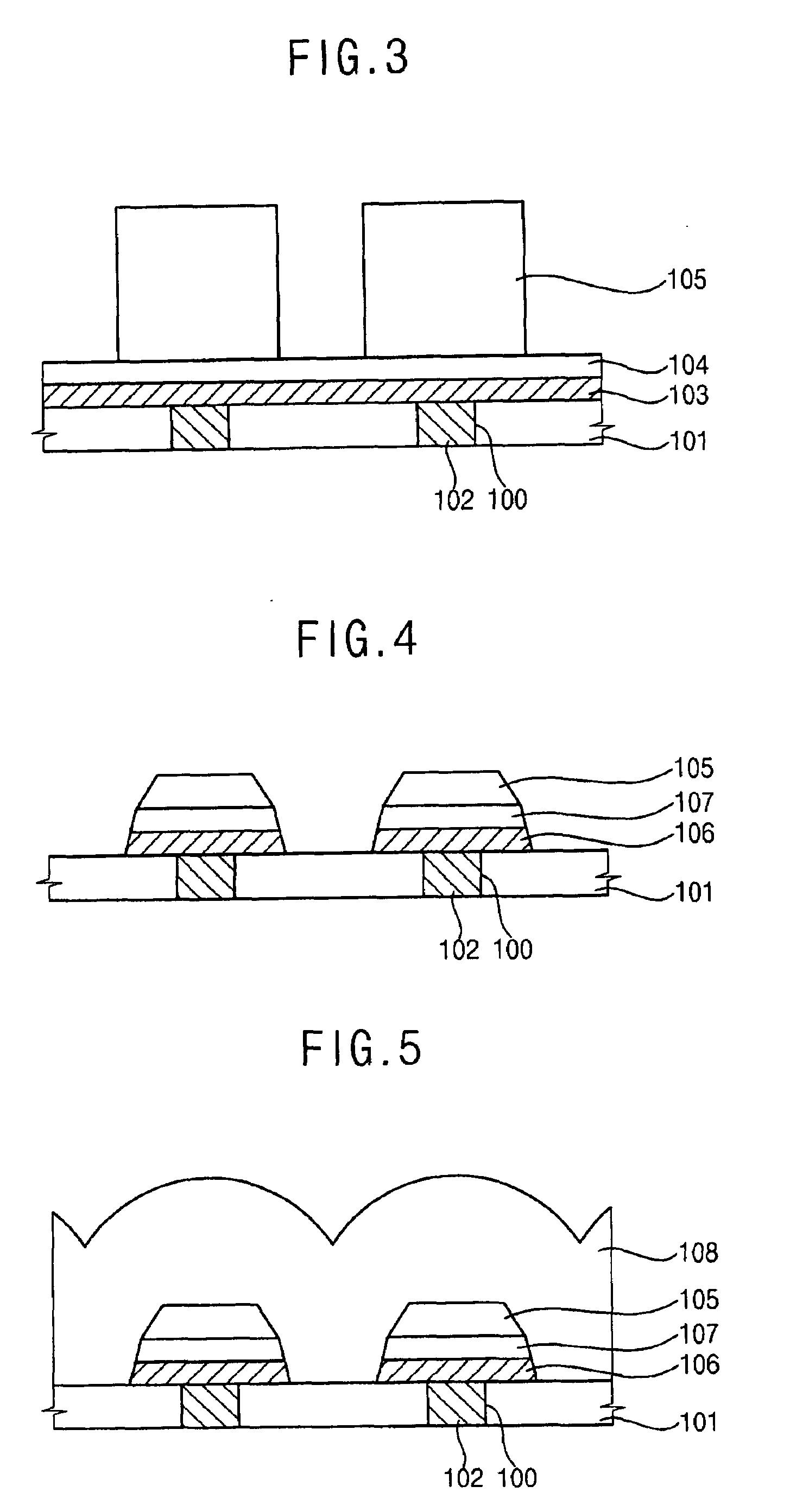
[0044]FIGS. 3-8 illustrate cross-sectional views of stages in a method of manufacturing a ferroelectric capacitor in accordance with the present invention. Referring to FIG. 3, a first insulating pattern 101 having a hole 100 may be formed on an underlying structure (not shown), and a contact structure 102 may be formed in the hole 100. An upper face of the first insulating pattern 101 may be substantially coplanar with an upper face of the contact structure 102.
[0045]A lower electrode layer 103 and a ferroelectric layer 104 may be successively formed on the first insulating pattern 101 and the contact structure 102. The ferroelectric layer 104 may include a ferroelectric material including titanium and oxygen. For example, the ferroelectric material may include one or more of PZT, SBT, BLT, PLZT, BST, etc.
[0046]A mask pattern 105 may be formed on the ferroelectric layer 104. The mask pattern 105 may be disposed over the contact structure 102. A width of the mask pattern 105 may be ...
third embodiment
[0055]FIGS. 9-15 illustrate cross-sectional views of stages in a method of manufacturing a ferroelectric capacitor in accordance with the present invention. Referring to FIG. 9, a first insulating pattern 201 having a hole 200 may be formed on an underlying structure (not shown), and a first conductive layer (not shown) may be formed in the hole 200. The first conductive layer may include, e.g., tungsten. The first conductive layer may be planarized until the first insulating pattern 201 is exposed, thereby forming a preliminary first contact (not shown) in the hole 200.
[0056]Where the preliminary first contact includes tungsten, dishing may occur at an upper portion of the preliminary first contact. Thus, a second contact 203 may be formed to prevent the dishing. In detail, an etch-back process may be performed on the preliminary first contact to remove an upper portion thereof, thereby transforming the preliminary first contact into a first contact 202. The first contact 202 may p...
PUM
 Abstract
Description
Claims
Application Information