
TSV layout structure and TSV interconnect structure, and fabrication methods thereof

a technology of layout structure and interconnect structure, applied in the direction of semiconductor/solid-state device details, semiconductor devices, electrical apparatus, etc., can solve the problems of copper residues on the mask layer, difficult to integrate more semiconductor devices in a two-dimensional (2d) package structure, and small semiconductor device dimensions

Active Publication Date: 2018-11-27
SEMICON MFG INT (SHANGHAI) CORP
View PDF6 Cites 1 Cited by
  • Summary
  • Abstract
  • Description
  • Claims
  • Application Information

AI Technical Summary

Benefits of technology

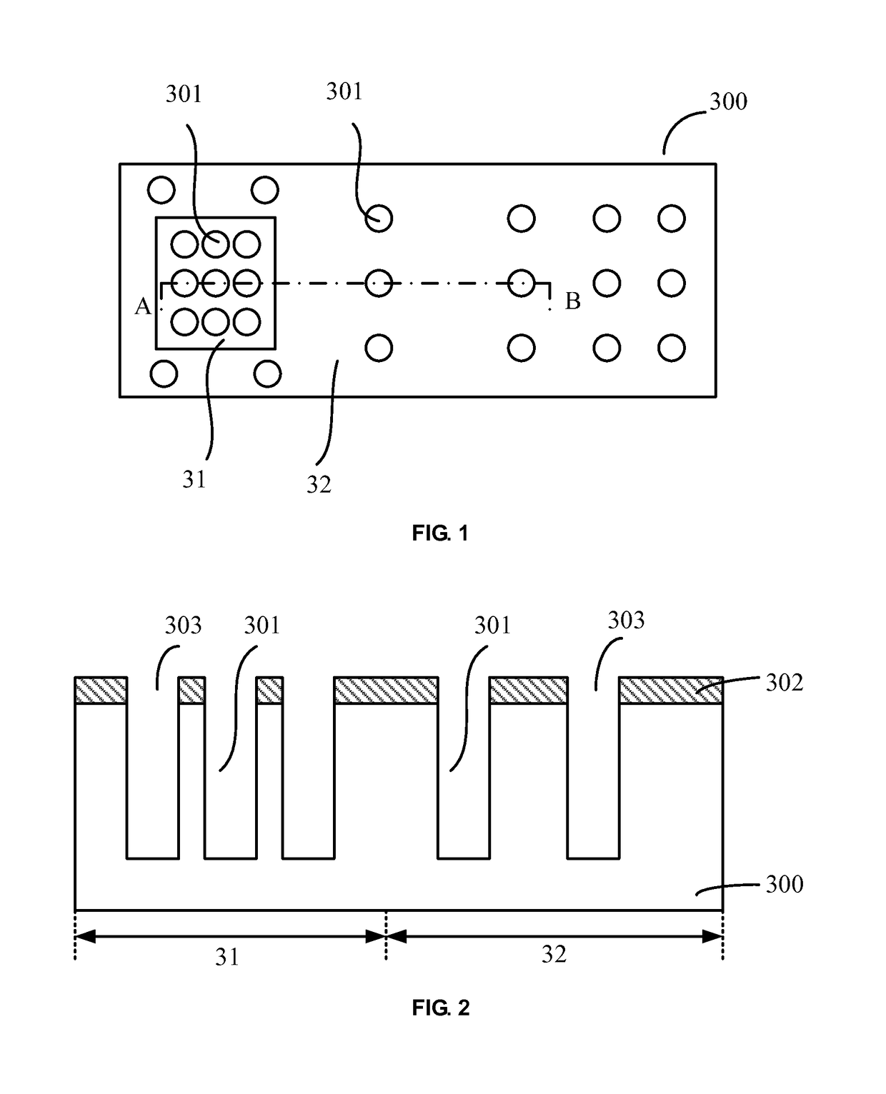
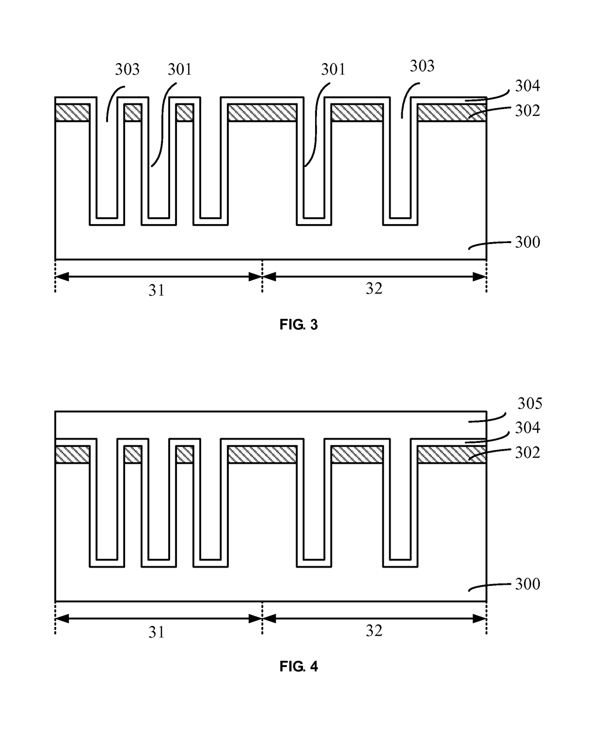
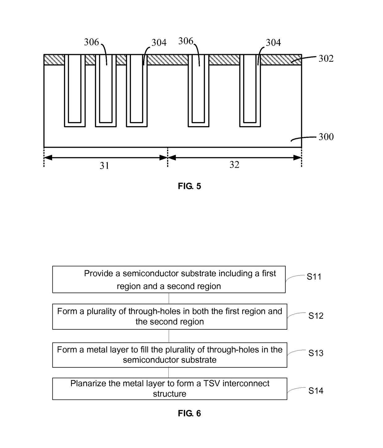
[0015]Disclosed herein provides TSV layout structures and TSV interconnect structures and methods of forming the TSV layout structures and the TSV interconnect structures. The difference in polishing rates due to the density difference of TSVs in different regions can be reduced during the chemical mechanical polishing process, e.g., by determining or controlling a relationship between an average density of TSVs in the semiconductor substrate and a density of TSVs in one region (e.g., a first region) of the semiconductor device. This can reduce or eliminate remaining metal residues after polishing and can provide surface uniformity of the TSV interconnect structure with enlarged latitude for processing.
[0012]When thinning a copper layer by a chemical mechanical process, the region with a high density of TSVs (e.g., having more TSVs on a unit area) tends to generate more copper residues on the surface than the region with a low density of TSVs (e.g., having less TSVs on a unit area). This can be because the region with a high density of TSVs contains more TSVs and thus more copper filled in the through vias. Material hardness of the region with a high density of TSVs can be smaller than the material hardness of the region with a low density of TSVs. The smaller the material hardness of a region, the smaller the friction force induced during the chemical mechanical polishing process and the lower the polishing rate of such region. Thus the polishing rate of the copper layer on the surface of the mask layer in a region with a high density of TSVs is lower than that on the surface of the mask layer in a region with a low density of TSVs, when the copper layer is removed from the surface of the mask layer by a chemical mechanical polishing process. A difference of polishing rates then occurs between the region with a high density of TSVs and the region with a low density of TSVs.
[0012]When thinning a copper layer by a chemical mechanical process, the region with a high density of TSVs (e.g., having more TSVs on a unit area) tends to generate more copper residues on the surface than the region with a low density of TSVs (e.g., having less TSVs on a unit area). This can be because the region with a high density of TSVs contains more TSVs and thus more copper filled in the through vias. Material hardness of the region with a high density of TSVs can be smaller than the material hardness of the region with a low density of TSVs. The smaller the material hardness of a region, the smaller the friction force induced during the chemical mechanical polishing process and the lower the polishing rate of such region. Thus the polishing rate of the copper layer on the surface of the mask layer in a region with a high density of TSVs is lower than that on the surface of the mask layer in a region with a low density of TSVs, when the copper layer is removed from the surface of the mask layer by a chemical mechanical polishing process. A difference of polishing rates then occurs between the region with a high density of TSVs and the region with a low density of TSVs.

Problems solved by technology

The critical dimension (CD) of semiconductor devices becomes very small along the development of semiconductor technology, and integrating more semiconductor devices in a two dimensional (2D) package structure becomes much more difficult.
However, when thinning the copper layer by the chemical mechanical polishing, copper residues often remain on the mask layer.
This affects stability of the formed copper interconnect structure.

Method used


Image

  • TSV layout structure and TSV interconnect structure, and fabrication methods thereof
  • TSV layout structure and TSV interconnect structure, and fabrication methods thereof
  • TSV layout structure and TSV interconnect structure, and fabrication methods thereof

Examples


Embodiment Construction

[0011]Reference will now be made in detail to exemplary embodiments of the disclosure, which are illustrated in the accompanying drawings. Wherever possible, the same reference numbers will be used throughout the drawings to refer to the same or like parts.

[0012]When thinning a copper layer by a chemical mechanical process, the region with a high density of TSVs (e.g., having more TSVs on a unit area) tends to generate more copper residues on the surface than the region with a low density of TSVs (e.g., having less TSVs on a unit area). This can be because the region with a high density of TSVs contains more TSVs and thus more copper filled in the through vias. Material hardness of the region with a high density of TSVs can be smaller than the material hardness of the region with a low density of TSVs. The smaller the material hardness of a region, the smaller the friction force induced during the chemical mechanical polishing process and the lower the polishing rate of such region....


PUM


Abstract

TSV layout structure and TSV interconnect structure, and their fabrication methods are provided. An exemplary TSV interconnect structure includes a semiconductor substrate having a first region and a second region; and a plurality of through-holes disposed in the first region and the second region of the semiconductor substrate. An average through-hole density of the first region is greater than an average through-hole density of the entire semiconductor substrate. The average through-hole density of the entire semiconductor substrate is less than or equal to about 2%. A metal layer having a planarized surface is filled in the plurality of through-holes in the semiconductor substrate.

Description

CROSS-REFERENCES TO RELATED APPLICATIONS[0001]This application claims priority to Chinese Patent Application No. CN201310106719.9, filed on Mar. 28, 2013, the entire contents of which are incorporated herein by reference.FIELD OF THE DISCLOSURE[0002]The present disclosure generally relates to the field of semiconductor manufacturing technology and, more particularly, relates to TSV (i.e., through silicon via) layout structures and TSV interconnect structures and methods of fabricating the TSV layout structures and the TSV interconnect structures.BACKGROUND[0003]The critical dimension (CD) of semiconductor devices becomes very small along the development of semiconductor technology, and integrating more semiconductor devices in a two dimensional (2D) package structure becomes much more difficult. A three dimensional package structure becomes an effective way to achieve a higher integration. The 3D package technology includes: die stacking and package stacking, both based on gold wire...

Claims


Application Information

Patent Timeline
Patent Type & Authority Patents(United States)
IPC IPC(8): H01L21/44H01L23/48H01L21/768
CPCH01L23/481H01L21/76898H01L2924/0002H01L2924/00
Inventor ZHANG, WUZHICHEN, XIAOJUNLIU, XUANJIEZHANG, HAIFANG
Owner SEMICON MFG INT (SHANGHAI) CORP
Learn More