

TSV layout structure and TSV interconnect structure, and fabrication methods thereof
a technology of layout structure and interconnect structure, applied in the direction of semiconductor/solid-state device details, semiconductor devices, electrical apparatus, etc., can solve the problems of copper residues on the mask layer, difficult to integrate more semiconductor devices in a two-dimensional (2d) package structure, and small semiconductor device dimensions
- Summary
- Abstract
- Description
- Claims
- Application Information
AI Technical Summary
Benefits of technology
Problems solved by technology
Method used
Image

Examples
Embodiment Construction
[0011]Reference will now be made in detail to exemplary embodiments of the disclosure, which are illustrated in the accompanying drawings. Wherever possible, the same reference numbers will be used throughout the drawings to refer to the same or like parts.
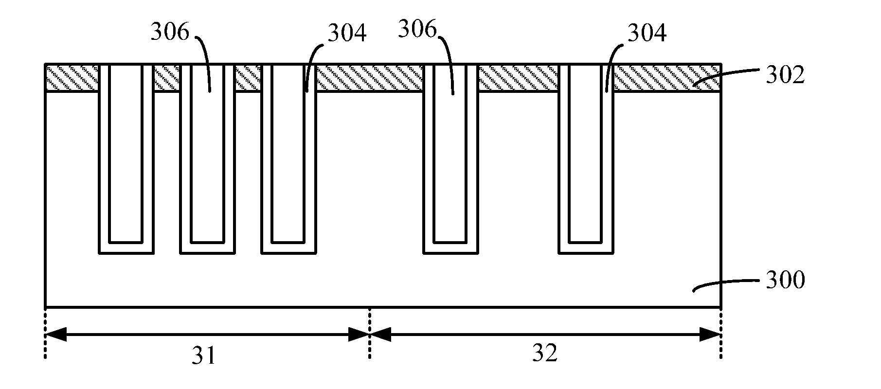
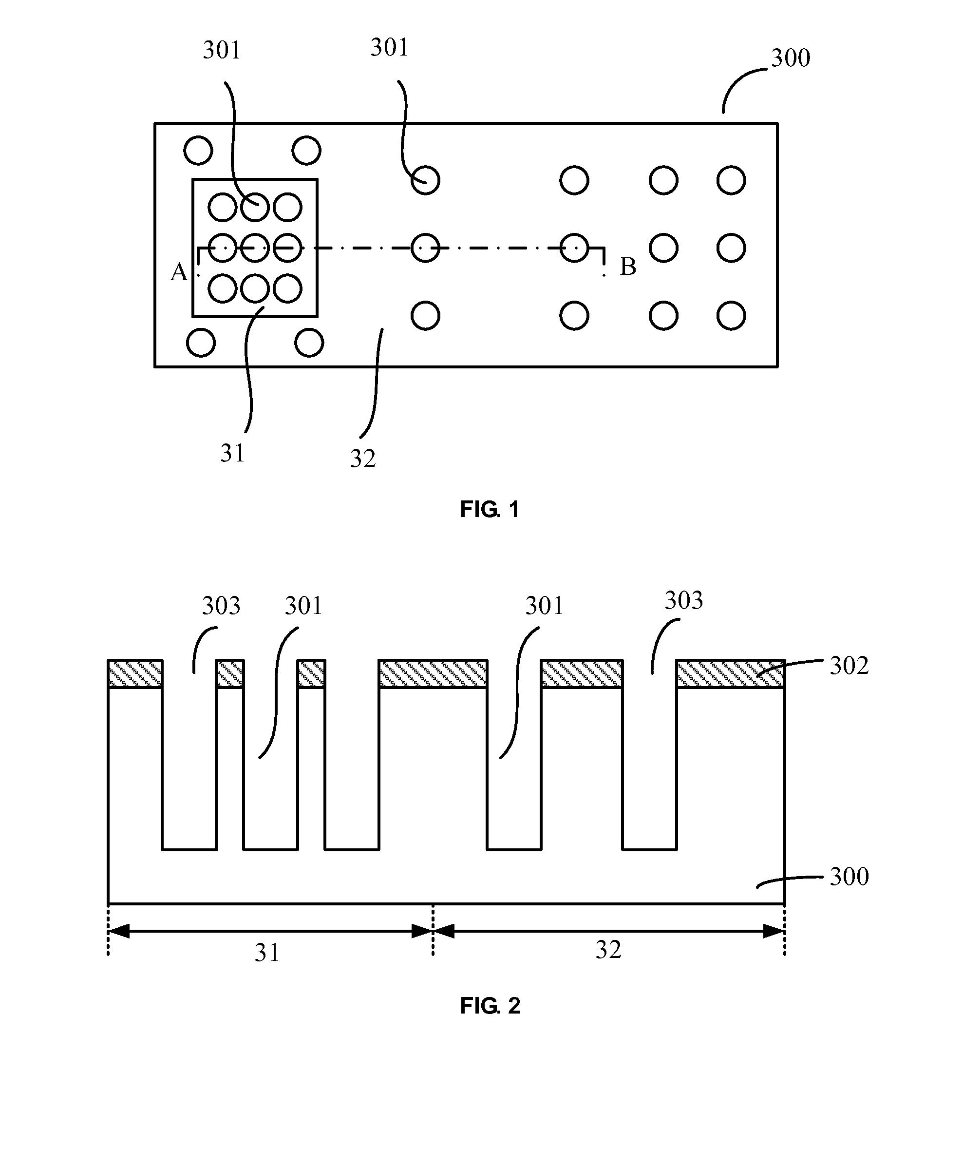
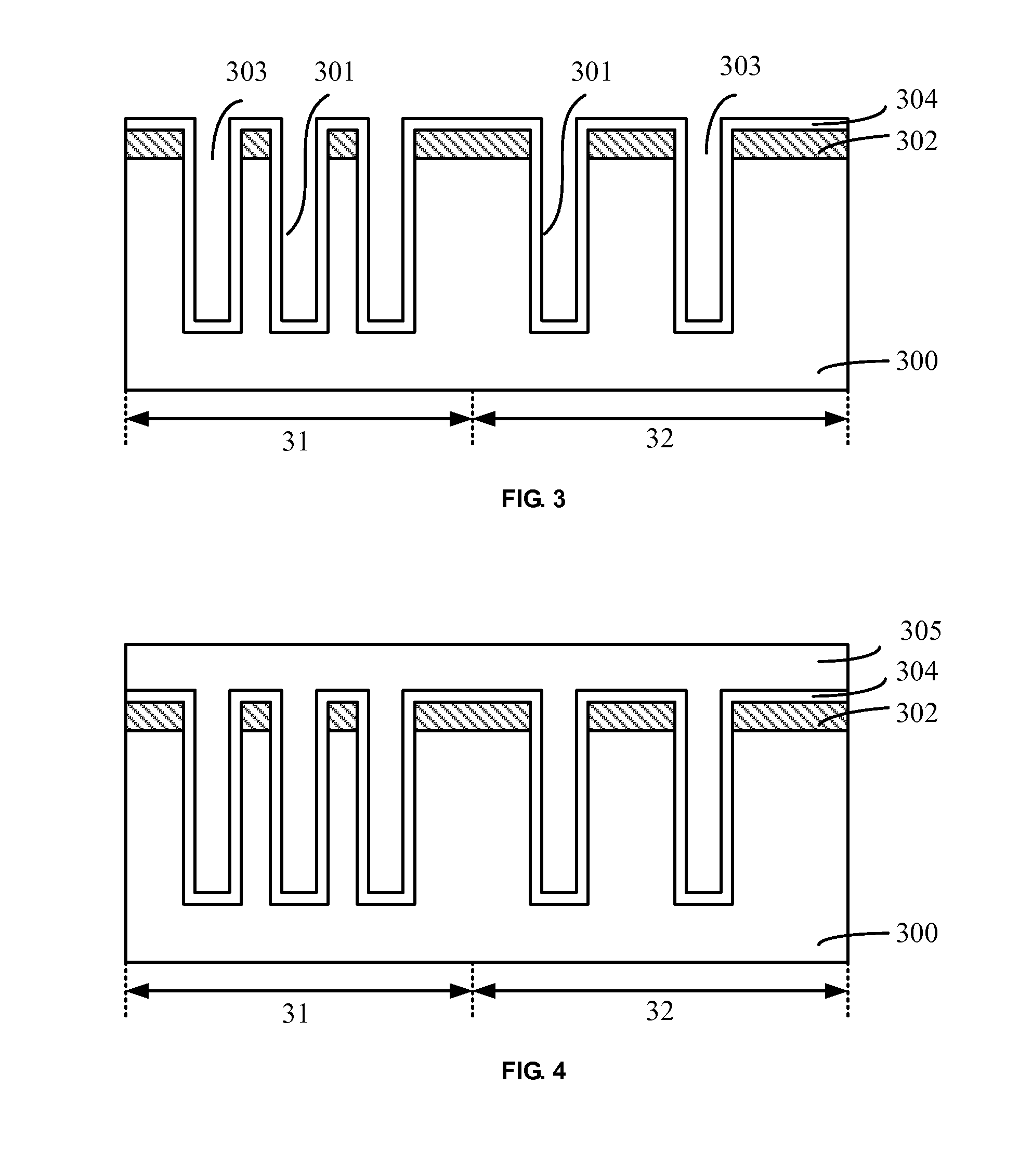
[0012]When thinning a copper layer by a chemical mechanical process, the region with a high density of TSVs (e.g., having more TSVs on a unit area) tends to generate more copper residues on the surface than the region with a low density of TSVs (e.g., having less TSVs on a unit area). This can be because the region with a high density of TSVs contains more TSVs and thus more copper filled in the through vias. Material hardness of the region with a high density of TSVs can be smaller than the material hardness of the region with a low density of TSVs. The smaller the material hardness of a region, the smaller the friction force induced during the chemical mechanical polishing process and the lower the polishing rate of such region....
PUM
 Abstract
Description
Claims
Application Information