
White organic light emitting device

a light-emitting device and organic technology, applied in the direction of organic semiconductor devices, solid-state devices, semiconductor devices, etc., can solve the problems of difficult multiple-use shadow masks, poor internal quantum efficiency of fluorescent elements,

Active Publication Date: 2015-10-13
LG DISPLAY CO LTD
View PDF12 Cites 4 Cited by
  • Summary
  • Abstract
  • Description
  • Claims
  • Application Information

AI Technical Summary

Benefits of technology

[0017]One object of the present invention is to provide a white organic light emitting device which has high color temperature and improved change in color coordinates according to luminance change.
[0026]The first electron transport layer may include at least two electron transport layers, one of the at least two electron transport layers may be formed of a material minimizing diffusion of a metal from the first light emitting layer, and the other of the at least two electron transport layers may be formed of an organic material enabling electron injection through doping with a metal.

Problems solved by technology

However, if the shadow mask is used in a large area, the shadow mask sags due to load thereof, and thus it is difficult to use the shadow mask multiple times, and an error occurs during formation of an organic light emitting layer pattern.
Further, the fluorescent elements have poor internal quantum efficiency and thus have white color coordinate properties in which red is strongly displayed.

Method used


Image

  • White organic light emitting device
  • White organic light emitting device
  • White organic light emitting device

Examples


Embodiment Construction

[0042]Reference will now be made in detail to the preferred embodiments of the present invention, examples of which are illustrated in the accompanying drawings. Wherever possible, the same reference numbers will be used throughout the drawings to refer to the same or like parts.

[0043]Hereinafter, an exemplary embodiment of the present invention will be described in detail with reference to FIGS. 1 to 10.

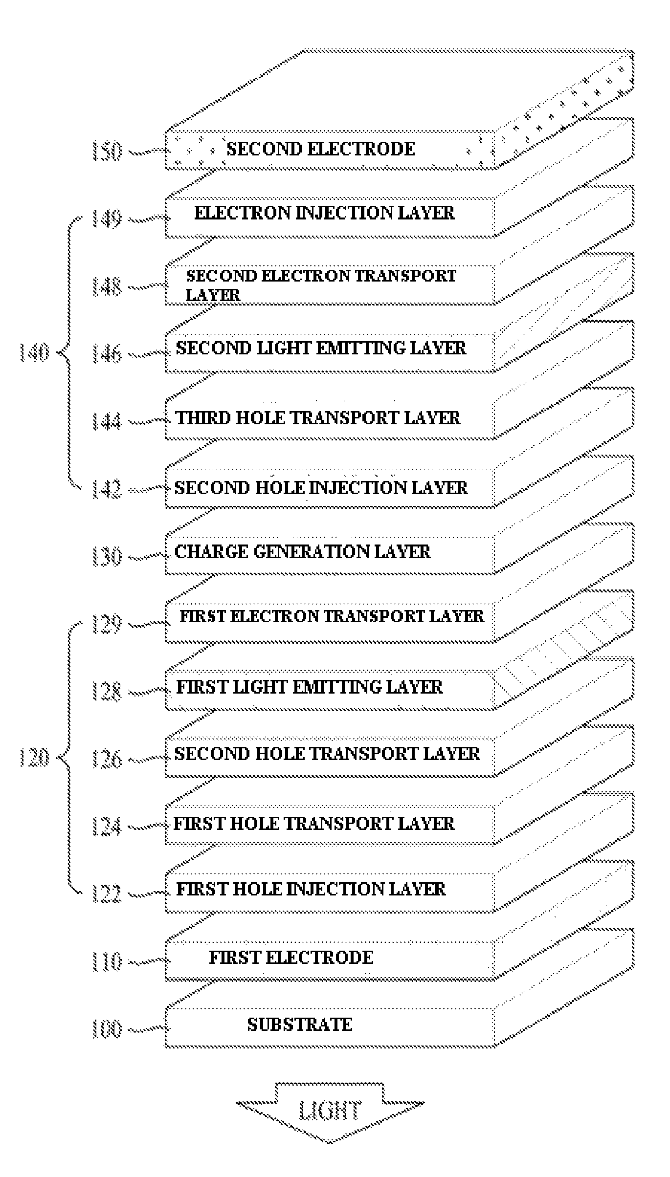
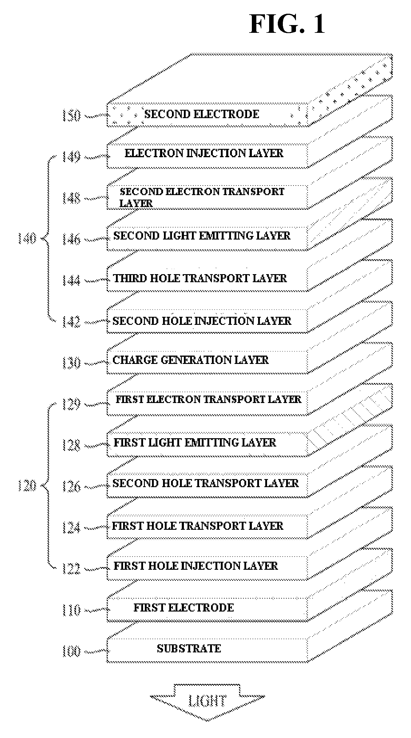
[0044]FIG. 1 is a perspective view illustrating a white organic light emitting device in accordance with one embodiment of the present invention.

[0045]With reference to FIG. 1, the white organic light emitting device in accordance with the embodiment of the present invention includes a first electrode 110 and a second electrode 150 opposite to each other on a substrate 100, and a first stack 120, a charge generation layer (CGL) 130 and a second stack 140 stacked between the first electrode 110 and the second electrode 150.

[0046]The first electrode 110 serving as an anode may be form...


PUM


Abstract

A white organic light emitting device which has high color temperature characteristics and no change in color coordinates according to luminance change, includes a first electrode and a second electrode opposite to each other on a substrate, a charge generation layer formed between the first electrode and the second electrode, a second stack including a second light emitting layer formed between the charge generation layer and the second electrode, and a first stack including a first light emitting layer formed between the first electrode and the charge generation layer, wherein the first emitting layer has low singlet-triplet exchange energy to change triplet excitons into a singlet state by triplet-triplet annihilation and a dopant concentration of the first light emitting layer is adjusted according to a luminance change curve of the second stack.

Description

[0001]This application claims the benefit of Korean Patent Application No. 10-2010-0104975, filed on Oct. 26, 2010, which is hereby incorporated by reference as if fully set forth herein.BACKGROUND OF THE INVENTION[0002]1. Field of the Invention[0003]The present invention relates to a white organic light emitting device, and more particularly, to a white organic light emitting device which has high color temperature characteristics and improved change in color coordinates according to luminance change.[0004]2. Discussion of the Related Art[0005]Recently, as the information age has arrived in earnest, a display field to visually express electric information signals has rapidly developed. In order to satisfy such a trend, various flat display devices having excellent performance, such as a thin profile, a light weight, and low power consumption, have been developed and have quickly replaced conventional cathode ray tube displays.[0006]Examples of the flat display devices include liqui...

Claims


Application Information

Patent Timeline
Patent Type & Authority Patents(United States)
IPC IPC(8): H01L51/50H01L51/52H01L27/32
CPCH01L51/5278H01L27/3209H01L51/504H01L2251/5376H01L51/508H01L51/5076H10K59/32H10K50/13H10K50/165H10K50/166H10K50/19H10K2101/27
Inventor PIEH, SUNG-HOONKIM, CHANG-OHSONG, KI-WOOG
Owner LG DISPLAY CO LTD
Learn More