

Organic electroluminescence device capable of simulating sunlight and preparation method thereof
A technology of luminescence and sunlight, which is applied in the field of organic electroluminescent devices simulating sunlight and its preparation, can solve the problems of increased preparation process requirements, repeatability effects, and complicated device structures, and achieve low preparation process requirements, The effect of simple process and simple structure
- Summary
- Abstract
- Description
- Claims
- Application Information
AI Technical Summary
Problems solved by technology
Method used
Image

Examples
Embodiment 1
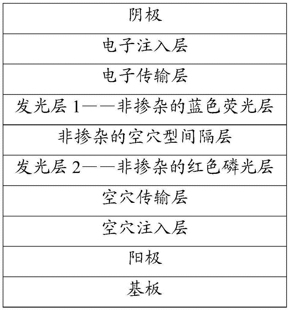
[0099] An organic electroluminescence device A for simulating sunlight, the structure of the device A is: ITO / HAT-CN(100nm) / NPB(15nm) / TAPC(5nm) / Ir(piq) 3 (0.5nm) / TAPC(1.5nm) / Ir(dmppy) 2 (dpp)(0.9nm) / TAPC(3.5nm) / DSA-ph(0.5nm) / TmPyPB(35nm) / LiF(1nm) / Al(200nm).
[0100] Such as Figure 4 As shown, the structure of the device A is sequentially stacked by the following functional layers:
[0101] Substrate, anode, hole injection layer, hole transport layer, red phosphorescent layer, phosphorescent spacer layer, yellow phosphorescent layer, spacer layer, blue fluorescent layer, electron transport layer, electron injection layer, cathode.
[0102] The aforementioned substrate is glass.
[0103] The above-mentioned anode is an ITO thin film.
[0104] The above-mentioned hole injection layer is a 100 nm thick HAT-CN thin film.
[0105] The above-mentioned hole transport layer includes a hole transport layer 1 and a hole transport layer 2 laminated in sequence, the hole transport la...
Embodiment 2
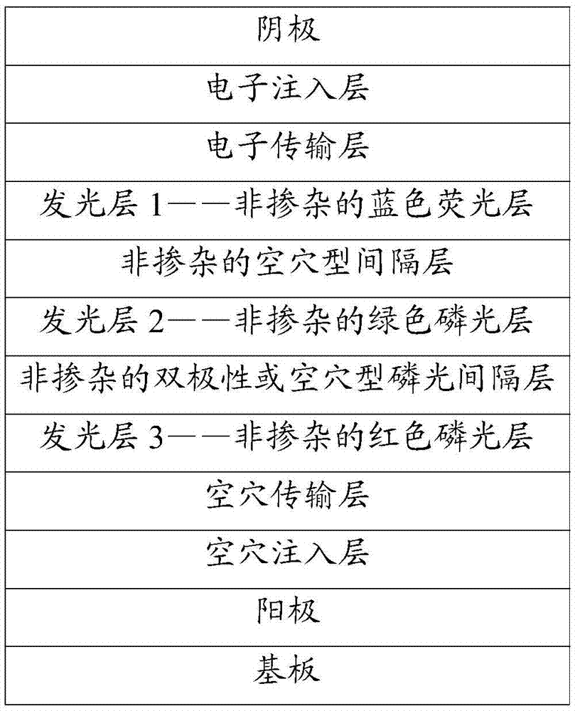
[0130] An organic electroluminescence device simulating sunlight, the organic electroluminescence device B, the structure of the device B is: ITO / HAT-CN(100nm) / NPB(15nm) / TAPC(5nm) / Ir(piq) 3 (0.2nm) / Ir(ppy) 3 (0.5nm) / TAPC(3.5nm) / DSA-ph(0.5nm) / TmPyPB(35nm) / LiF(1nm) / Al(200nm).
[0131] Such as Figure 6 As shown, the structure of the device B is sequentially stacked by the following functional layers:
[0132] Substrate, anode, hole injection layer, hole transport layer, red phosphorescent layer, green phosphorescent layer, spacer layer, blue fluorescent layer, electron transport layer, electron injection layer, cathode.
[0133] The aforementioned substrate is glass.
[0134] The above-mentioned anode is an ITO thin film.
[0135] The above hole injection layer is a 60nm thick HAT-CN thin film.
[0136] The above-mentioned hole transport layer includes a hole transport layer 1 and a hole transport layer 2 laminated in sequence, the hole transport layer 1 is a NPB film with ...
PUM
| Property | Measurement | Unit |
|---|---|---|
| Thickness | aaaaa | aaaaa |
| Thickness | aaaaa | aaaaa |
| Thickness | aaaaa | aaaaa |
Abstract
Description
Claims
Application Information