Semiconductor light-emitting device and manufacturing method

a technology of semiconductors and light-emitting devices, which is applied in the direction of semiconductor/solid-state device manufacturing, semiconductor devices, electrical devices, etc., can solve the problems of color variability in structure, and achieve the effects of uniform color tone, small light-emitting surface, and high light-emitting efficiency

Active Publication Date: 2013-08-01
STANLEY ELECTRIC CO LTD
View PDF5 Cites 15 Cited by
  • Summary
  • Abstract
  • Description
  • Claims
  • Application Information

AI Technical Summary

Benefits of technology

[0025]According to the above-described exemplary semiconductor light-emitting device, the device can emit a wavelength converted light from the top surface of the transparent plate that is smaller than the top surface of the semiconductor light-emitting chip while the reflective layer can be used as a reflector that extends from the side surface of the semiconductor light-emitting chip toward the side surface of the transparent plate and contacts with the bottom surface of the light-emitting chip. In this case, light excited by light emitted in a crosswise direction of the semiconductor light-emitting chip can be reflected on the side concave surface of the reflective layer, and can be directed toward a central region of the top surface of the transparent plate. The exited light directed toward the central region can be mixed with light having an original wavelength emitted along the optical axis of the device in light emitted from the chip, and therefore a color temperature on the central region of the light-emitting surface can increase and a color temperature on an outer region can reduce as compared with conventional devices. Thus, the disclosed subject matter can provide semiconductor light-emitting devices that can emit a wavelength converted light having a substantially uniform color tone and a high light-emitting efficiency from a very small light-emitting surface.
[0028]According to the exemplary manufacturing method described above for the semiconductor light-emitting devices, the reflective layer used as the reflector can be formed by disposing an uncured reflective material between the frame and the both side surfaces of the wavelength converting layer and the transparent plate and between the bottom surface of the semiconductor light-emitting chip and the mounting surface of the base board. The wavelength converting material and the reflective material can be solidified by a similar method as compared to conventional processes. Thus, the method can provide semiconductor light-emitting devices having a substantially uniform color tone, a high light-emitting efficiency and a small light-emitting surface using manufacturing machines that are similar to those used to manufacture conventional semiconductor light-emitting devices.

Problems solved by technology

However, in the conventional light-emitting device, such structure may be subject to color variability in the wavelength converted light.

Method used


Image

  • Semiconductor light-emitting device and manufacturing method
  • Semiconductor light-emitting device and manufacturing method
  • Semiconductor light-emitting device and manufacturing method

Examples


first embodiment

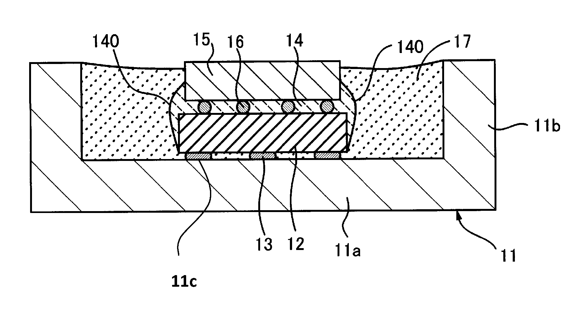
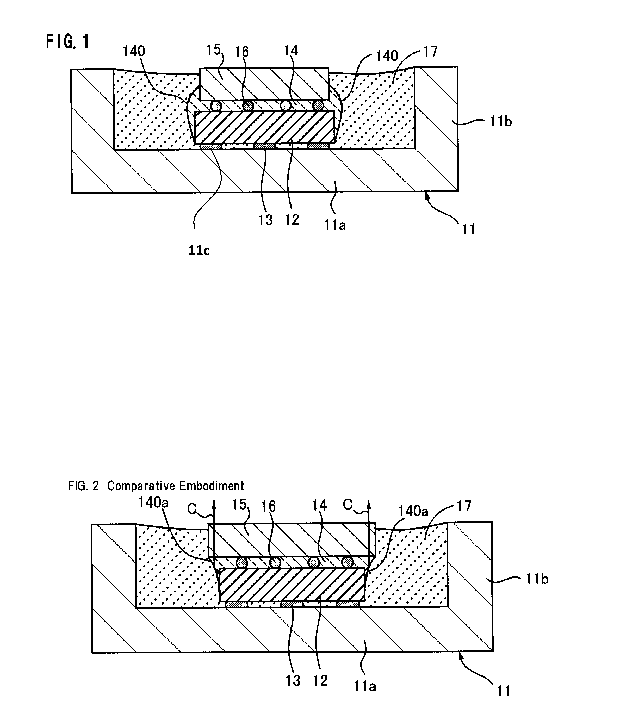
[0065]In the first embodiment shown in FIG. 1, in order to avoid covering the top surface of the transparent plate 15 with the reflective layer 17, the reflective layer 17 is disposed in the cavity of the casing 11 so that the top surface thereof is lower than the top surface of the transparent plate 15. However, the top surface of the reflective layer 17 should not be limited to the above-described position. If the reflective layer 17 does not cover the part of the top surface of the transparent plate 15, the reflective layer 17 can be disposed in the cavity of the casing 11 at the same level as the top surface of the transparent plate 15.

[0066]According to the semiconductor light-emitting device having the above-described structure, light emitted in an upward direction from the semiconductor light-emitting chip 12 can enter into the wavelength converting layer 14, and a wavelength converted light can be emitted from the top surface of the transparent plate 15, which is the light-e...

second embodiment

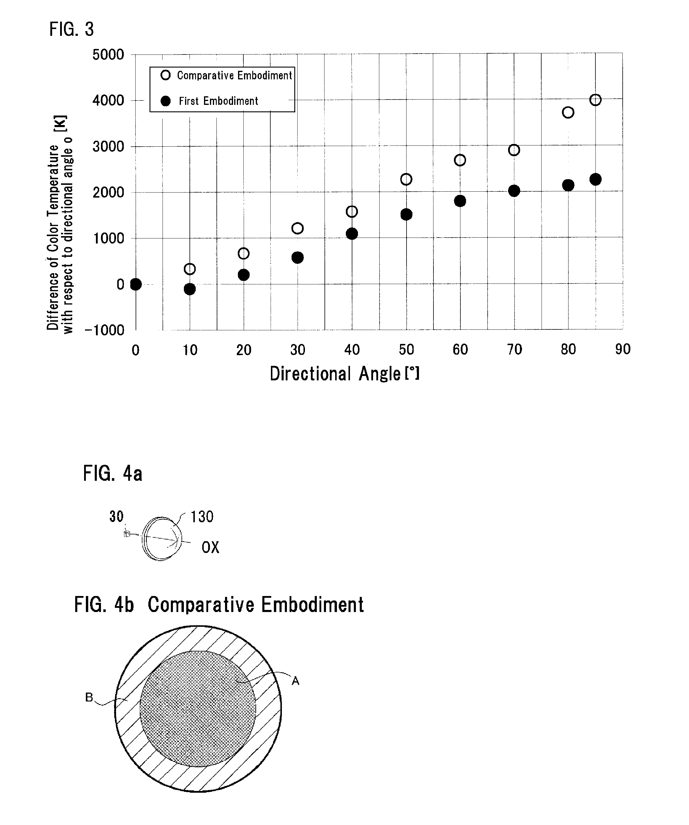
[0077]It has been well known that a lighting technology for beautifully showing goods laid out in a show window is difficult. One of the reasons is because it may be difficult for a lighting unit to illuminate the goods in a wide show window with light having a uniform color tone and with a small structure such that customers do not notice the illumination light. However, according to the semiconductor light-emitting device of the second embodiment as shown in FIG. 4a, the semiconductor light-emitting device can emit various wavelength converted lights having a substantially uniform color tone with a wide range for the show window and with a simple structure by using the projector lens 130.

[0078]In addition, the second embodiment can be used as a basic structure for a direct projector typed headlight without a reflector. Specifically, light emitted from the semiconductor light-emitting device 30 can be projected in reverse with respect to a vertical line via the projector lens 130. ...


PUM

PropertyMeasurementUnit
peak wavelengthaaaaaaaaaa
wavelengthaaaaaaaaaa
thicknessaaaaaaaaaa

Abstract

A semiconductor light-emitting device and a method for manufacturing the same can include a wavelength converting layer located on at least one semiconductor light-emitting chip in order to emit various colored lights including white light. The semiconductor light-emitting device can include a casing having a cavity and a mounting surface, the chip mounted on the mounting surface, a transparent plate mounted on the wavelength converting layer within a top surface of the chip and a reflective layer located in the cavity so as to surround the transparent plate, the wavelength converting layer and the chip. The semiconductor light-emitting device can be configured to improve light-colored variability and light-emitting efficiency of the chip by using the reflective layer as a reflector, and therefore can emit a wavelength-converted light having a substantially uniform color tone and a high light-emitting efficiency from a smaller light-emitting surface than the top surface of the chip.

Description

[0001]This application claims the priority benefit under 35 U.S.C. §119 of Japanese Patent Application No. 2012-013760 filed on Jan. 26, 2012, which is hereby incorporated in its entirety by reference.BACKGROUND[0002]1. Field[0003]The presently disclosed subject matter relates to semiconductor light-emitting devices in which light emitted from a semiconductor light-emitting chip is wavelength-converted by a wavelength converting layer, and to manufacturing methods for the same. More particularly, the disclosed subject matter relates to semiconductor light-emitting devices for a vehicle light and the like, which can emit various color lights having a substantially uniform color tone and a high light-emitting efficiency from a small light-emitting surface, and to methods of manufacturing such devices.[0004]2. Description of the Related Art[0005]Semiconductor light-emitting devices, in which a part of the light emitted from a semiconductor light-emitting chip is converted into light ha...

Claims


Application Information

Patent Timeline
Patent Type & Authority Applications(United States)
IPC IPC(8): H01L33/50H01L27/15
CPCH01L27/15H01L33/50H01L33/60H01L33/505H01L2224/13H01L33/58H01L2933/0041H01L2933/005H01L33/54
Inventor MOCHIZUKI, MIKA
Owner STANLEY ELECTRIC CO LTD
Why Eureka
Try Eureka