Photovoltaic cell with light trapping for enhanced efficiency

a photovoltaic cell and light trapping technology, applied in the field of thin film photovoltaic cells, can solve the problems of limiting the range of applications for which photovoltaic cells are used, relative inefficiency of photovoltaic cells, etc., to achieve the effect of enhancing photovoltaic conversion efficiency, increasing the penetration of incident light, and increasing the total path length

Active Publication Date: 2015-11-17
NAT TECH & ENG SOLUTIONS OF SANDIA LLC
View PDF1 Cites 4 Cited by
  • Summary
  • Abstract
  • Description
  • Claims
  • Application Information

AI Technical Summary

Benefits of technology

[0011]Another physical mechanism that is under study for enhancing photovoltaic conversion efficiency is the trapping of light within the photovoltaic semiconductor film. In contrast to approaches such as those described above which aim at increasing the penetration of incident light into the film, trapping-based approaches aim to increase the total path length traversed by incident photons while they remain within the film. Trapping is advantageous for several reasons: For a given film thickness, it increases the probability of bandgap absorption events, which can lead to higher photovoltaic conversion efficiency. It also permits the use of a film whose thickness is less than its intrinsic absorption length. This is advantageous because in at least some materials of practical interest, thinner films tend to be more efficient in the collection of photogenerated carriers.

Problems solved by technology

The relative inefficiency of photovoltaic cells has been one significant factor limiting the range of applications for which photovoltaic cells are a commercially viable source of alternative energy.
One cause of inefficiency is reflection, across the pertinent part of the solar spectrum, from the front surface of the semiconductor film that contains the photovoltaic junction region.

Method used


Image

  • Photovoltaic cell with light trapping for enhanced efficiency
  • Photovoltaic cell with light trapping for enhanced efficiency
  • Photovoltaic cell with light trapping for enhanced efficiency

Examples


example i

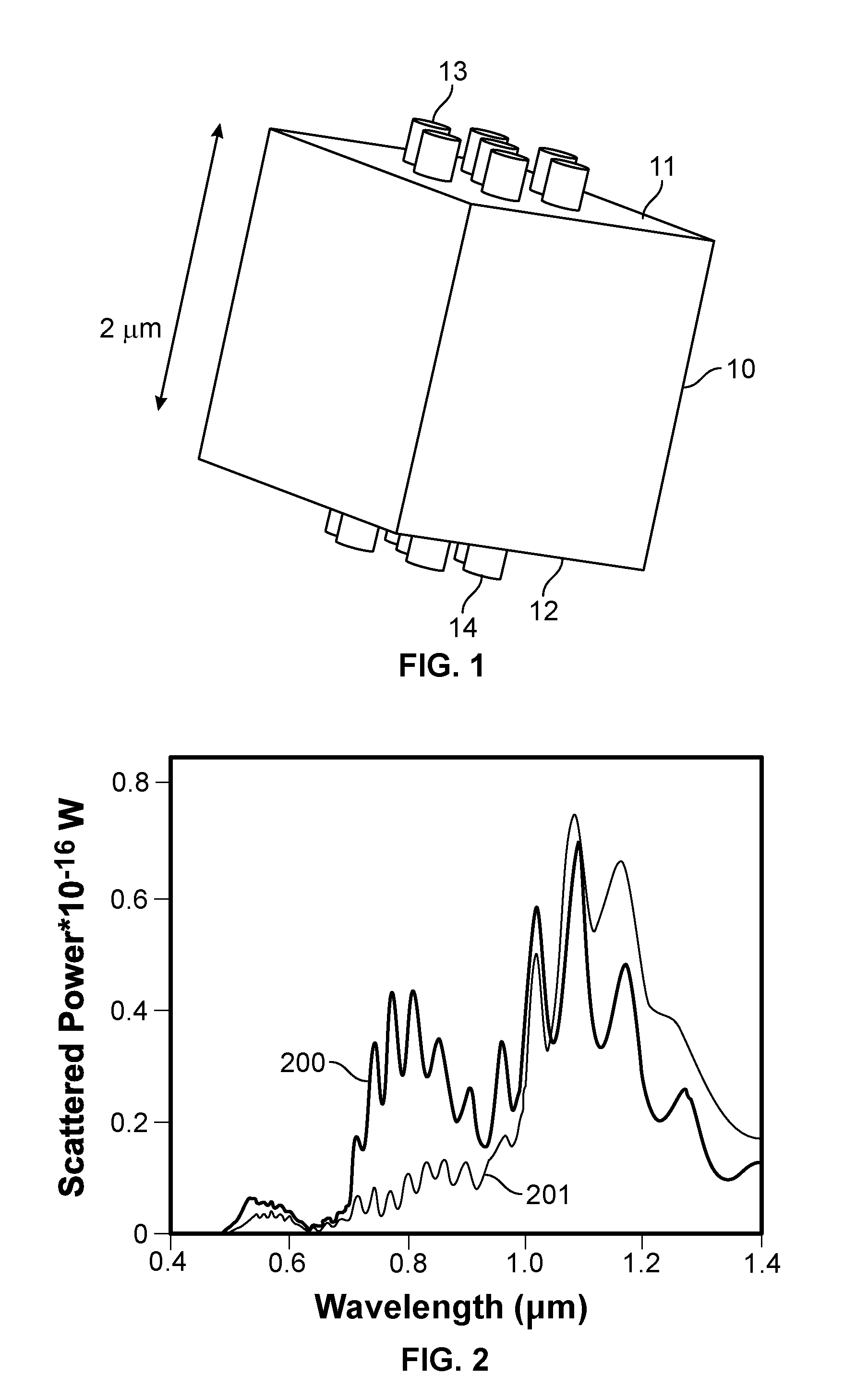
[0056]We performed FDTD modeling as described above. Three scenarios were modeled as shown in FIG. 5: Scenario A was the isolated nanocylinder, Scenario B was the silicon film with front-surface nanocylinder impinged from air, and Scenario C was the silicon film with back-surface cylinder impinged from within the silicon film.

[0057]FIGS. 6-8 provide polar plots of the angular distribution of the scattered power at a resonance wavelength of 800 nm for scenarios A and B (FIGS. 6 and 7 respectively) and at a resonance wavelength of 900 nm for scenario C (FIG. 8). The source is polarized in one of the two principal directions.

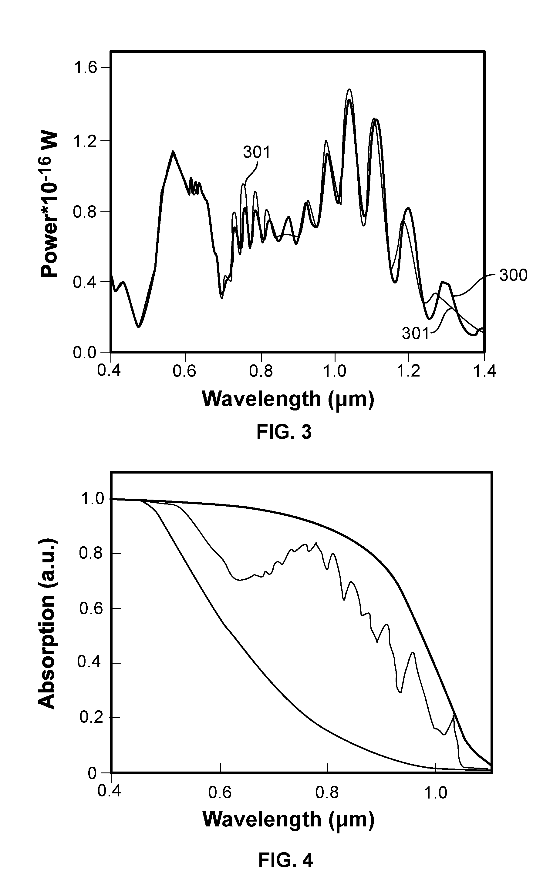
[0058]The polar plot of the scattered power for scenario A at a wavelength of 800 nm clearly indicates electric dipole scattering characteristics.

[0059]It is important to note that for Scenarios B (wavelength at 800 nm) and C (wavelength at 900 nm), the resonances are hybrids of electric and magnetic dipole modes. They are not pure electric dipole modes as in Scena...

example ii

[0062]In an alternate embodiment, an array of nanocylinders is created on the front surface of the silicon layer. Instead of a back-surface nanocylinder array, a metallic mirror is created on the back surface of the silicon layer. In essence, the reflective image of the front-side antireflection array serves as the back-side trapping array.

[0063]This simplifies the fabrication process, since only one side of the photovoltaic cell needs to be patterned with nanostructures. Moreover, the metallic array, which may be made, e.g., from deposited silver or aluminum, can also be used for the back-side electrode.

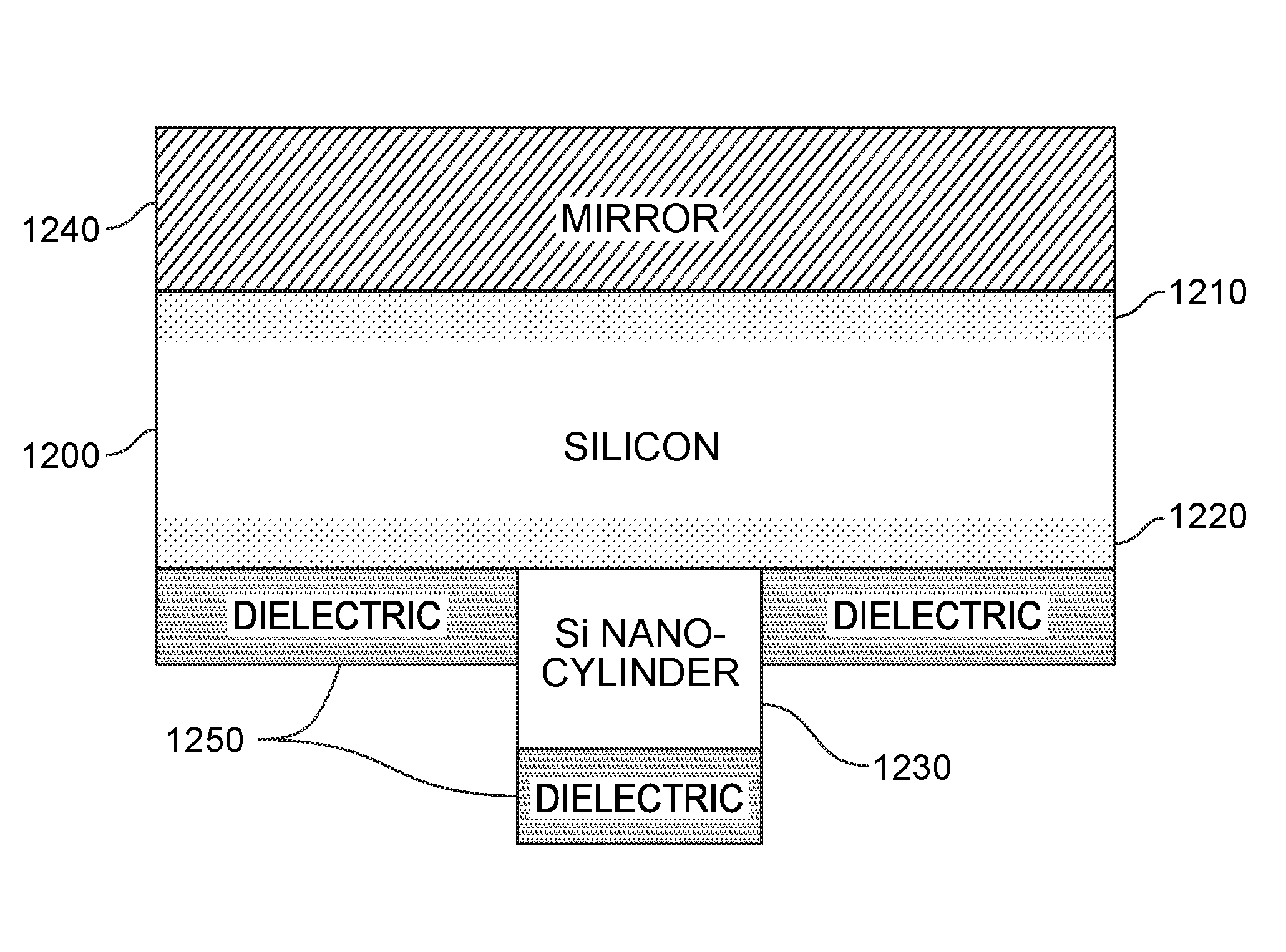
[0064]We performed numerical simulations to predict the performance of such an arrangement. The simulated structure is illustrated in FIG. 12. As seen, the structure includes silicon layer 1200, which has a doped region 1210 near the back surface and an oppositely doped region 1220 near the front surface. One silicon nanocylinder 1230 is shown formed on the front surface of the sili...


PUM


Abstract

The efficiency of a photovoltaic cell is enhanced by light trapping using Mie-scattering nanostructures. In one embodiment, an array of nanocylinders is formed on the front surface of a silicon film to enhance forward scattering into the film, and an array of nanocylinders is formed on the back surface to enhance backscattering so that more light is absorbed within the silicon film. In an alternate embodiment, a mirror layer is formed on the back surface of the silicon film to reflect light within the film back toward the front-surface nanocylinder array.

Description

CROSS-REFERENCE TO RELATED APPLICATION[0001]This application claims priority to U.S. Provisional Patent Application No. 61 / 909,422, filed on Nov. 27, 2013 under the title, “ENHANCING EFFICIENCY IN THIN FILM SILICON SOLAR CELLS”, the entirety of which is incorporated herein by reference.STATEMENT OF GOVERNMENT RIGHTS[0002]This invention was made with Government support under Contract No. DE-AC04-94AL85000 awarded by the U.S. Department of Energy. The Government has certain rights in the invention.FIELD OF THE INVENTION[0003]The invention relates to thin-film photovoltaic cells, and more particularly to the modification of the surfaces of thin-film photovoltaic cells to increase efficiency. Still more particularly, the invention relates to surface-modified thin-film silicon photovoltaic cells.ART BACKGROUND[0004]The relative inefficiency of photovoltaic cells has been one significant factor limiting the range of applications for which photovoltaic cells are a commercially viable sourc...

Claims


Application Information

Patent Timeline
Patent Type & Authority Patents(United States)
IPC IPC(8): H01L33/00H01L31/0216H01L31/056
CPCH01L31/02168H01L31/056H01L31/02327Y02E10/52
Inventor BRENER, IGALFOFANG, NCHE TUMASANGLUK, TING S.
Owner NAT TECH & ENG SOLUTIONS OF SANDIA LLC
Why Eureka
Try Eureka