Optoelectronic platform with carbon based conductor and quantum dots and transistor comprising such a platform

a technology of optoelectronic platforms and quantum dots, applied in the field of optoelectronic platforms, can solve the problems of low-cost detectors, limited quantum efficiency, and limited read-out nois

Active Publication Date: 2016-01-12
FUNDACIO INST DE CIENCIES FOT NIQUES
View PDF11 Cites 5 Cited by
  • Summary
  • Abstract
  • Description
  • Claims
  • Application Information

AI Technical Summary

Problems solved by technology

However they are limited by read-out noise and their quantum efficiency is limited to unity (i.e. 1 carrier per absorbed photon).
The technological challenges in integrating these structures to common image sensors and low-cost detectors is the high operating bias required (on the order of 100's of V) and additional layers required to suppress leakage currents and prolong the device lifetime from degradation due to the high applied bias.
Moreover, these devices are not monolithically integrable to CMOS electronics due to the different growth process required for APDs.

Method used


Image

  • Optoelectronic platform with carbon based conductor and quantum dots and transistor comprising such a platform
  • Optoelectronic platform with carbon based conductor and quantum dots and transistor comprising such a platform
  • Optoelectronic platform with carbon based conductor and quantum dots and transistor comprising such a platform

Examples


Embodiment Construction

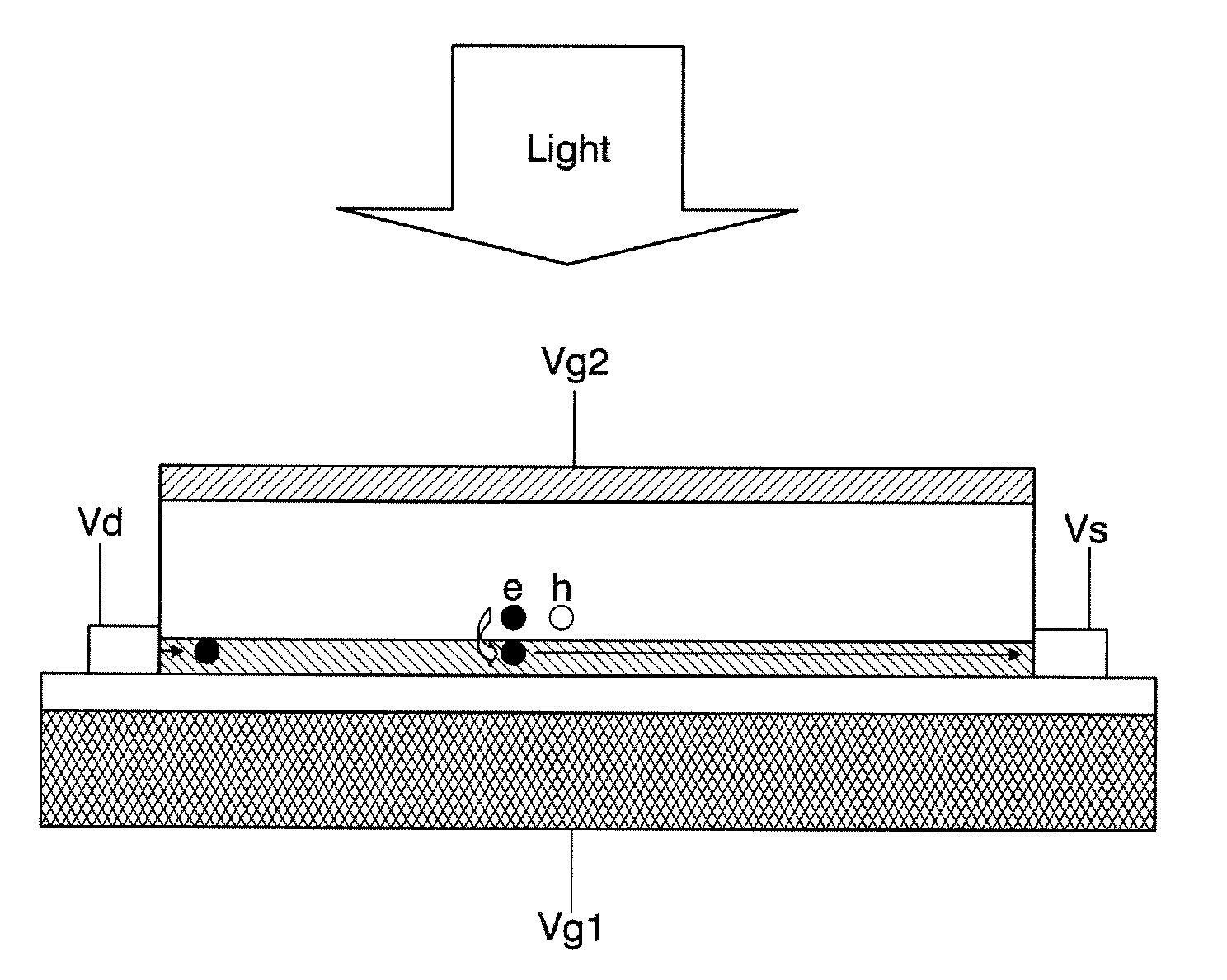
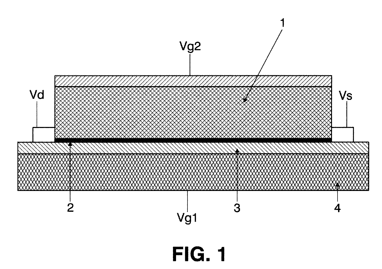
[0011]The invention is an hybrid optoelectronic platform compatible with CMOS integration, which consists of a carbon based layer (for example graphene) sensitized with colloidal quantum dots (CQDs). The carbon based layer is used as the carrier transport channel, and CQDs are employed as the absorbing material. As shown in FIG. 1, when applied to a phototransistor, a graphene layer (2) is deposited on a silicon substrate (4) with a SiO2 interlayer (3) to form the gate of the phototransistor, and two electrodes are connected to the graphene in the lateral dimension (Vs, Vd) to form the metal contacts of the device analogously to a source and drain electrodes in a FET transistor. Graphene is then overcoated with a layer of CQDs (1) whose bandgap can be tuned according to the size and material of the QDs (CdSe: 400-650 nm, PbS: 650-2000 nm, HgTe: 1500 nm-4000 nm).

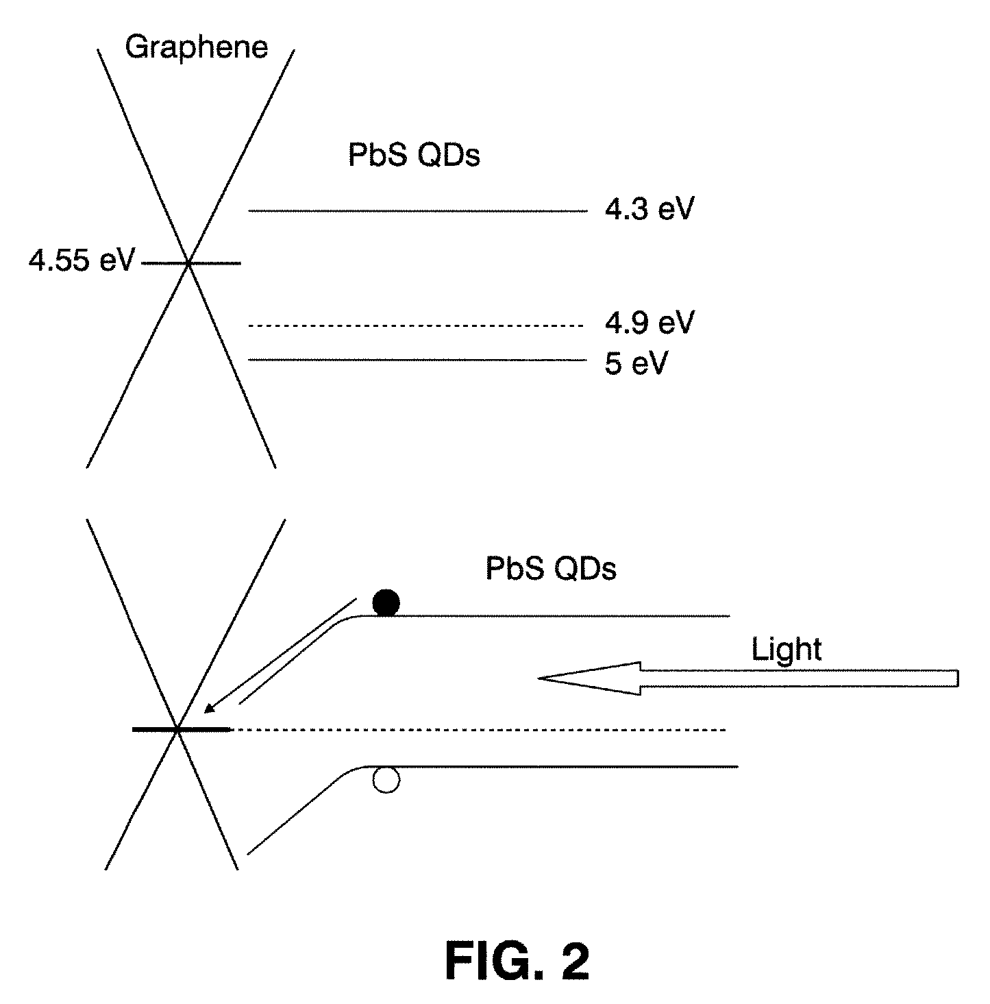
[0012]For the description of the underlying mechanism we focus in the case of PbS QDs, but this can be generally applied to...


PUM


Abstract

The invention comprises an optoelectronic platform with a carbon-based conduction layer and a layer of colloidal quantum dots on top as light absorbing material. Photoconductive gain on the order of 106 is possible, while maintaining de operating voltage low. The platform can be used as a transistor.

Description

[0001]This application claims priority of Spanish Patent Application No. P 201131345, filed Aug. 2, 2011, the entire contents of which are hereby incorporated by reference into this application.FIELD OF THE INVENTION[0002]The present invention relates to optoelectronic platforms. In particular, to a platform where photoconductive gain is improved.BACKGROUND OF INVENTION[0003]Photodiodes (InGaAs for short-wavelength infrared and Si for visible and near infra-red applications) demonstrate high sensitivity. However they are limited by read-out noise and their quantum efficiency is limited to unity (i.e. 1 carrier per absorbed photon). In view of the absence of photoconductive gain in photodiodes, APDs (avalanche photodiodes) have been developed to provide gain via carrier multiplication effects. The gain in these devices is on the order of 100 to 1000 carriers per absorbed photon. The technological challenges in integrating these structures to common image sensors and low-cost detector...

Claims


Application Information

Patent Timeline
Patent Type & Authority Patents(United States)
IPC IPC(8): B82Y20/00B82Y10/00H01L29/06H01L29/16H01L51/42H01L29/423H01L51/00H01L31/0352
CPCB82Y10/00B82Y20/00H01L29/0665H01L29/0673H01L29/1606H01L29/42364H01L51/428H01L51/0048H01L51/4213Y02E10/549H01L31/028H01L31/035218H01L31/113H01L31/112H10K85/221H10K30/10H10K30/65H01L31/0256Y02E10/547
Inventor GERASIMOS, KONSTANTATOSFRANK, KOPPENS
Owner FUNDACIO INST DE CIENCIES FOT NIQUES
Why Eureka
Try Eureka