

Integrated split gate non-volatile memory cell and logic device
a logic device and split gate technology, applied in the field of semiconductor structure making methods, can solve the problems of inability to integrate non-volatile memories (nvms) with logic transistors, difficult integration of nvm transistors and logic transistors, and inability to use control gate over floating gate configurations. to achieve the effect of reliable nvm at such small scal
- Summary
- Abstract
- Description
- Claims
- Application Information
AI Technical Summary
Benefits of technology
Problems solved by technology
Method used
Image

Examples
Embodiment Construction
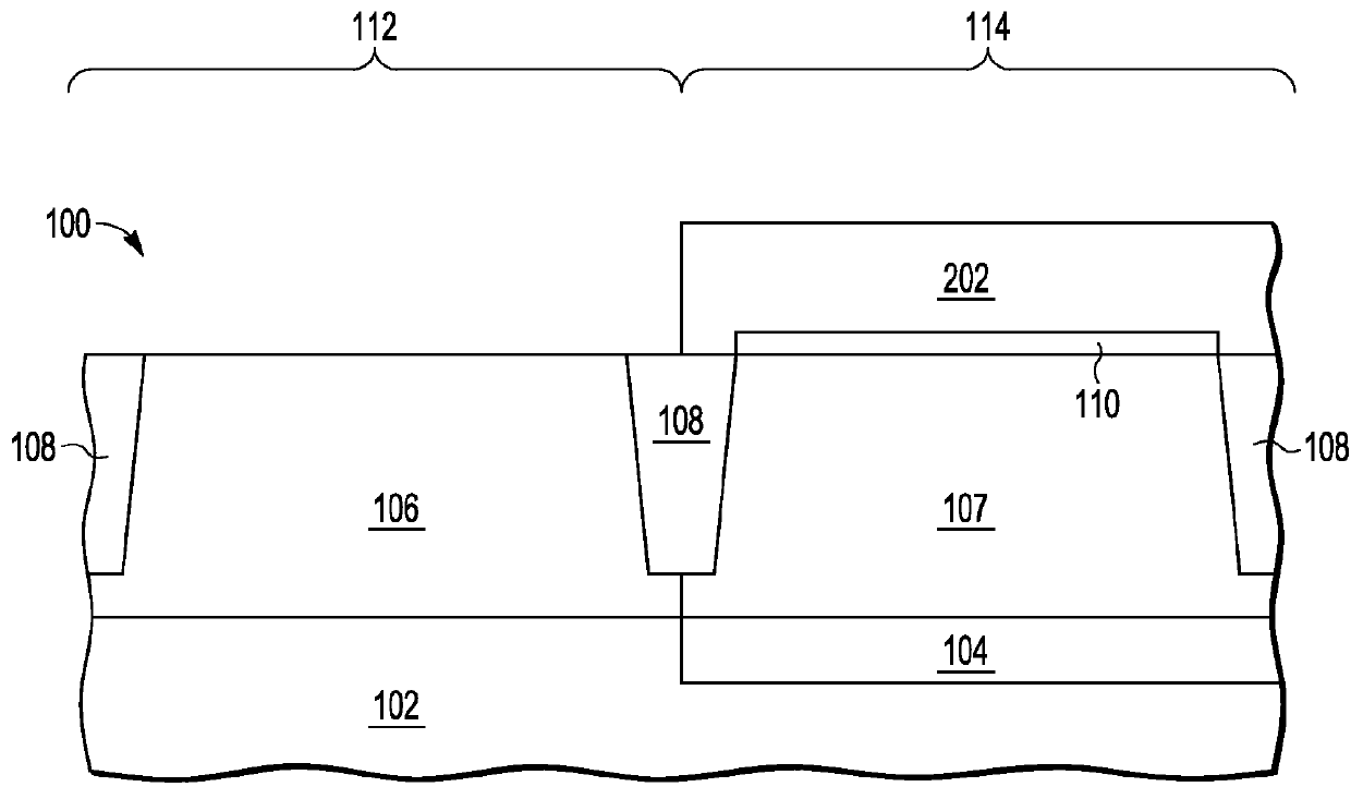
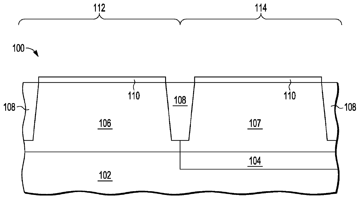
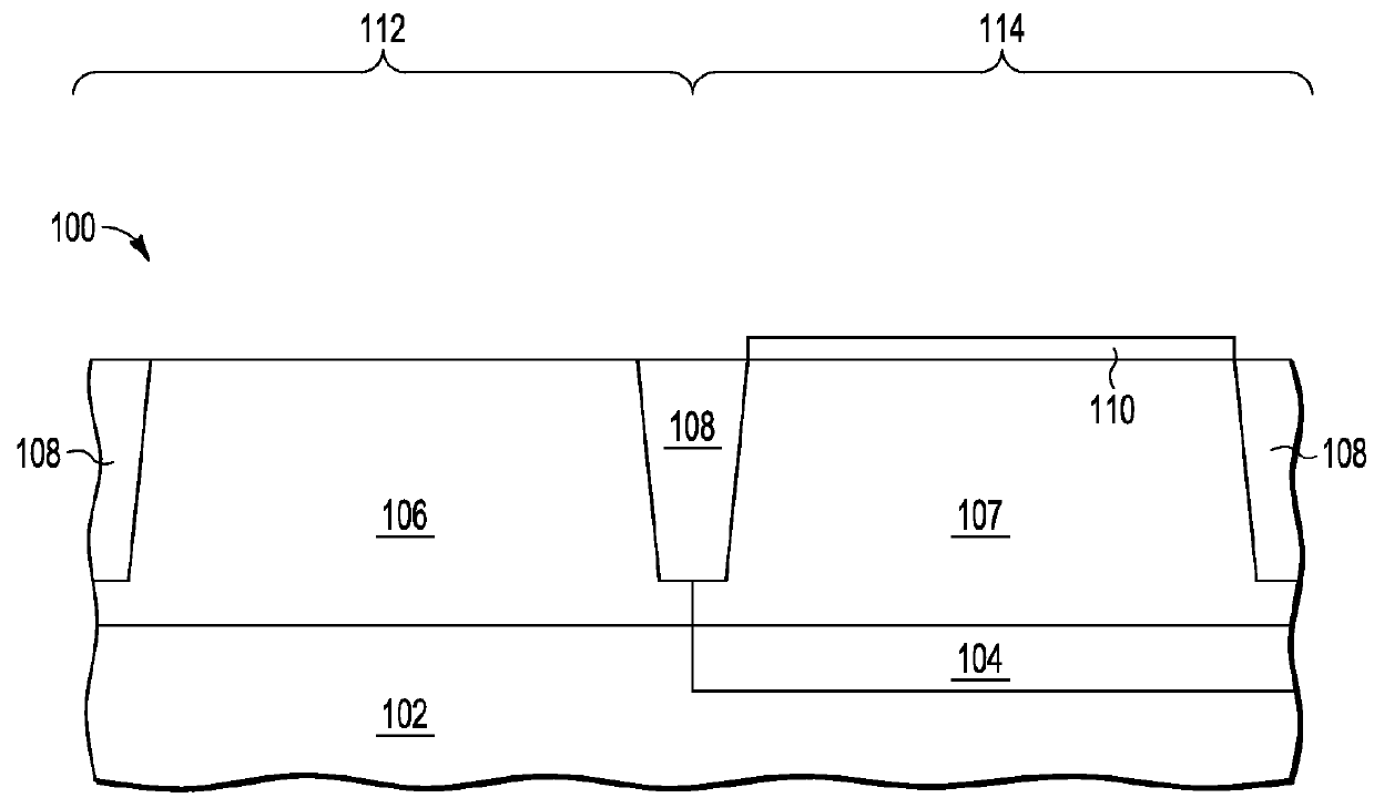
[0009]Embodiments of methods and structures for semiconductor structures including non-volatile memory (NVM) split gate memory cells integrated with logic devices such as transistors with high-k gate dielectric are disclosed. The split gate memory cells include a select gate and a control gate. Layers of oxide and nitride are deposited over a region of the substrate that includes the split gate structure while a gate stack that includes high-k dielectric is deposited over a region of the substrate where the logic devices are being formed. An interlayer dielectric over the NVM and logic regions can be chemically-mechanically polished during fabrication, which results in the control gate needing to become a spacer along one side of the select gate for the NVM. Metal gate material for the logic devices is deposited after the ILD is polished. This is better understood by reference to the following description and the drawings.
[0010]Shown in FIG. 1 is an embodiment of semiconductor struc...
PUM
 Abstract
Description
Claims
Application Information