Thin film transistor and manufacturing method thereof
- Summary
- Abstract
- Description
- Claims
- Application Information
AI Technical Summary
Benefits of technology
Problems solved by technology
Method used
Image


Examples
Embodiment Construction
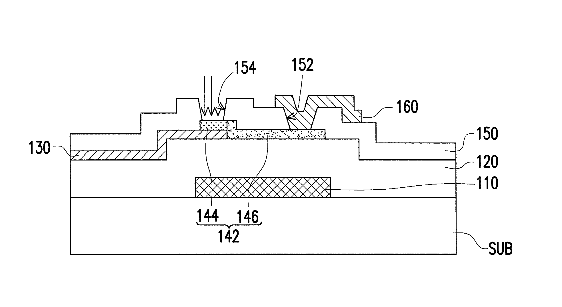
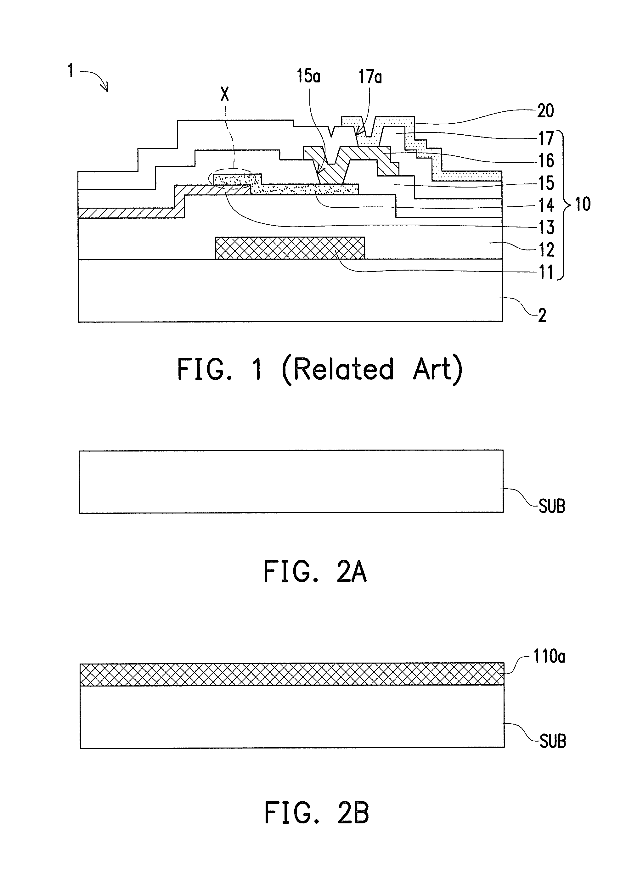
[0028]FIG. 2A through FIG. 2N are schematic cross-sectional views showing a manufacturing method of a thin film transistor according to an embodiment of the invention.
[0029]First, with reference to FIG. 2A, a substrate SUB is provided. In the present embodiment, a material of the substrate SUB may be an inorganic transparent material, an organic transparent material, an inorganic non-transparent material, an inorganic non-transparent material or the like. For instance, the substrate SUB may be a glass substrate, a plastic substrate or the like, but the substrate SUB of the present embodiment is not limited to be made of the aforementioned material. Additionally, the substrate SUB may be a rigid substrate or a flexible substrate.
[0030]Then, with reference to FIG. 2B through FIG. 2C′, a gate 110 is formed on the substrate SUB. In the present embodiment, the material of the gate 110, may be a metal, such as titanium, molybdenum, aluminum, an alloy thereof or a staking layer thereof. Du...
PUM
 Abstract
Description
Claims
Application Information
 - R&D
- Intellectual Property
- Life Sciences
- Materials
- Tech Scout
- Unparalleled Data Quality
- Higher Quality Content
- 60% Fewer Hallucinations
Browse by: Latest US Patents, China's latest patents, Technical Efficacy Thesaurus, Application Domain, Technology Topic, Popular Technical Reports.
© 2025 PatSnap. All rights reserved.Legal|Privacy policy|Modern Slavery Act Transparency Statement|Sitemap|About US| Contact US: help@patsnap.com