Nonvolatile memory and related reprogramming method

a nonvolatile memory and reprogramming technology, applied in the field of semiconductor memory devices, can solve problems such as reducing the operating margin of the device and being susceptible to errors, and achieve the effects of increasing the programming speed of the nonvolatile memory device, enhancing the read margin, and improving the threshold voltage distribution

Inactive Publication Date: 2016-03-08
SAMSUNG ELECTRONICS CO LTD
View PDF15 Cites 11 Cited by
  • Summary
  • Abstract
  • Description
  • Claims
  • Application Information

AI Technical Summary

Benefits of technology

[0008]These and other embodiments of the inventive concept may decrease a number of program pulses required in a reprogram operation and thus increase a programming speed of a nonvolatile memory device. They may also use time corresponding to the decrease of the program pulse for improving threshold voltage distributions and thus enhance a read margin.

Problems solved by technology

The storage of multiple bits per cell, however, tends to reduce the operating margins of the devices, rendering them susceptible to errors.

Method used


Image

  • Nonvolatile memory and related reprogramming method
  • Nonvolatile memory and related reprogramming method
  • Nonvolatile memory and related reprogramming method

Examples


Embodiment Construction

[0022]Embodiments of the inventive concept are described below with reference to the accompanying drawings. These embodiments are presented as teaching examples and should not be construed to limit the scope of the inventive concept.

[0023]In the description that follows, certain embodiments are described with respect to a flash memory device. However, the inventive concept can be applied to other forms of nonvolatile memory devices, such as PRAM, MRAM, ReRAM, FRAM, NOR flash memory, and others.

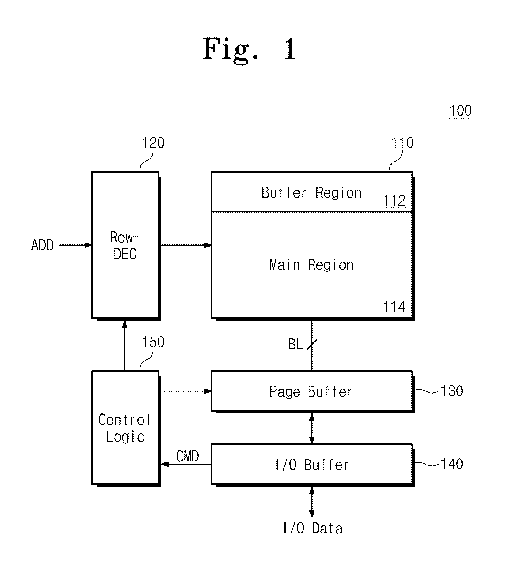
[0024]FIG. 1 is a block diagram of a nonvolatile memory device 100 according to an embodiment of the inventive concept.

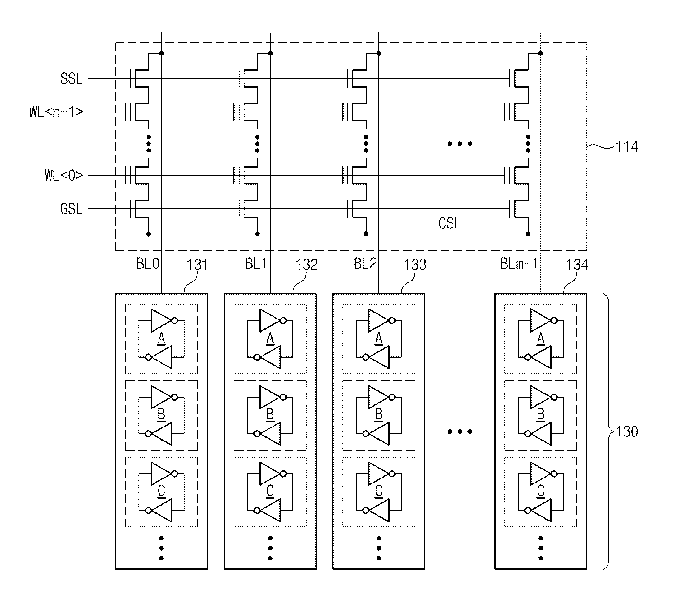
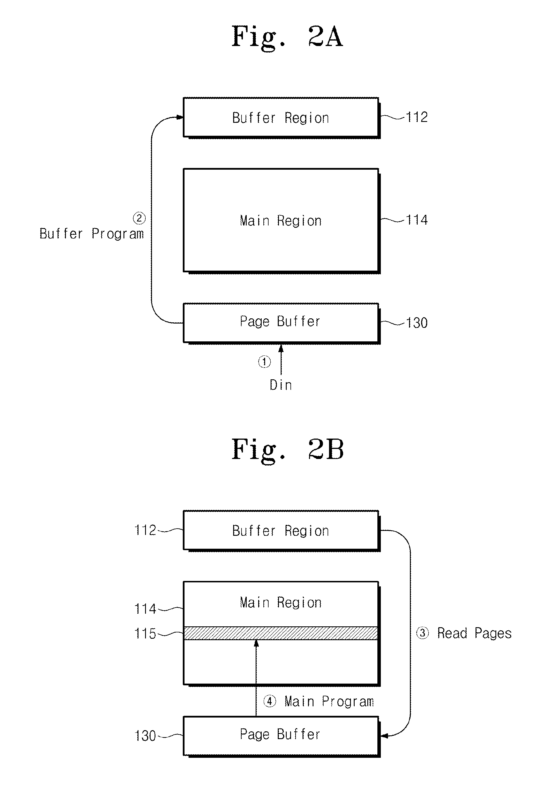
[0025]Referring to FIG. 1, nonvolatile memory device 100 comprises a cell array 110 having a buffer area 112 and a main area 114. Nonvolatile memory device 100 programs data stored in buffer area 112 to main area 114. Such a programming operation is referred to as an OBP operation.

[0026]Cell array 110 is connected to a row decoder 120 through wordlines (WLs) and selection line...


PUM


Abstract

A method of reprogramming a nonvolatile memory device, comprising setting up bit lines of selected memory cells according to logic values of first and second latches of a page buffer connected to the bit lines, supplying a program pulse to the selected memory cells, performing a program verify operation on the selected memory cells using the first and second latches, and performing a predictive program operation on the selected memory cells according to a result of the program verify operation. In the predictive program operation, bit lines of the selected memory cells are setup according to a logic value of a third latch of the page buffer that corresponds to each of the selected memory cells.

Description

CROSS-REFERENCE TO RELATED APPLICATIONS[0001]This application claims priority under 35 U.S.C. §119 to Korean Patent Application No. 10-2013-0059856 filed on May 27, 2013, the subject matter of which is hereby incorporated by reference.BACKGROUND OF THE INVENTION[0002]The inventive concept relates generally to semiconductor memory devices, and more particularly, to multi-level cell (MLC) nonvolatile memory devices and related reprogramming methods.[0003]Semiconductor memory devices can be roughly divided into two categories according to whether they retain stored data when disconnected from power. These categories include nonvolatile memory devices, which retain stored data when disconnected from power, and volatile memory devices, which lose stored data when disconnected from power.[0004]Flash memory devices are an increasingly popular form of nonvolatile memory devices. Flash memory devices are widely used to various forms of data (e.g., audio and images) in information appliances ...

Claims


Application Information

Patent Timeline
Patent Type & Authority Patents(United States)
IPC IPC(8): G11C16/04G11C16/34G11C11/56G11C16/10
CPCG11C16/107G11C11/5628G11C16/10G11C16/344G11C16/3459G11C16/34G06F12/0246G06F2212/7201G11C16/102G11C16/28
Inventor KIM, TAE-YOUNG
Owner SAMSUNG ELECTRONICS CO LTD
Why Eureka
Try Eureka