Laminate and method for manufacturing the same

a technology of laminate and manufacturing method, applied in the field of laminate, can solve the problems of low scratch resistance and durability, nano uneven structure body has lower scratch resistance, durability in use, etc., and achieve the effects of improving scratch resistance, excellent scratch resistance, and high restoration

Active Publication Date: 2016-03-22
MITSUBISHI CHEM CORP
View PDF11 Cites 1 Cited by
  • Summary
  • Abstract
  • Description
  • Claims
  • Application Information

AI Technical Summary

Benefits of technology

[0020]In the present invention, the intermediate layer has specific physical properties and a specific thickness, and the ratio of the thickness of the surface layer to that of the intermediate layer is in a specific range. Thereby, indentation flaws and recessed flaws tend to be well restored, which dramatically improves scratch resistance with respect to repeat scratch. The present invention exhibits “3H” or greater in a pencil hardness test according to JIS K5600-5-4.
[0021]In the present invention, the ratio of the storage modulus of the surface layer to that of the intermediate layer is in the specific range. Thereby, the laminate has high restoration with respect to strain caused by pressing, excellent scratch resistance, particularly high scratch resistance when the strain caused by pressing is repeated, excellent durability, a high antireflection function, and a good appearance.

Problems solved by technology

However, the surface of the nano uneven structure has a nanoscale projecting part which is apt to be inclined, and has lower scratch resistance and durability than a smooth surface made of the same resin.
The nano uneven structure body has lower scratch resistance than a molded product such as a hard coat produced using the same resin composition and having a smooth surface, and has a problem with durability in use.
However, the nano uneven structure bodies described in Patent Literatures 1 to 4 do not necessarily satisfy scratch resistance.
Even when the cured resin has hardness of “H” or greater in the pencil hardness test, the fine projection may be broken or bent to impair antireflective performance, particularly in the case of the nano uneven structure body, and the application thereof is limited.
Although the antireflective film described in Patent Literature 5 has the intermediate layer having a self-restoring function to dent caused by pressing, the antireflective film may exhibit insufficient scratch resistance.
When this is pushed in, the hard coat layer is broken, and is apt to be damaged in the pencil hardness test.

Method used


Image

  • Laminate and method for manufacturing the same
  • Laminate and method for manufacturing the same

Examples


examples

[0128]Hereinafter, the present invention will be specifically described with reference to Examples. The present invention is not limited thereto. In the following description, the term “parts” means “parts by mass” unless otherwise specified. Various measurements and valuation methods are as follows.

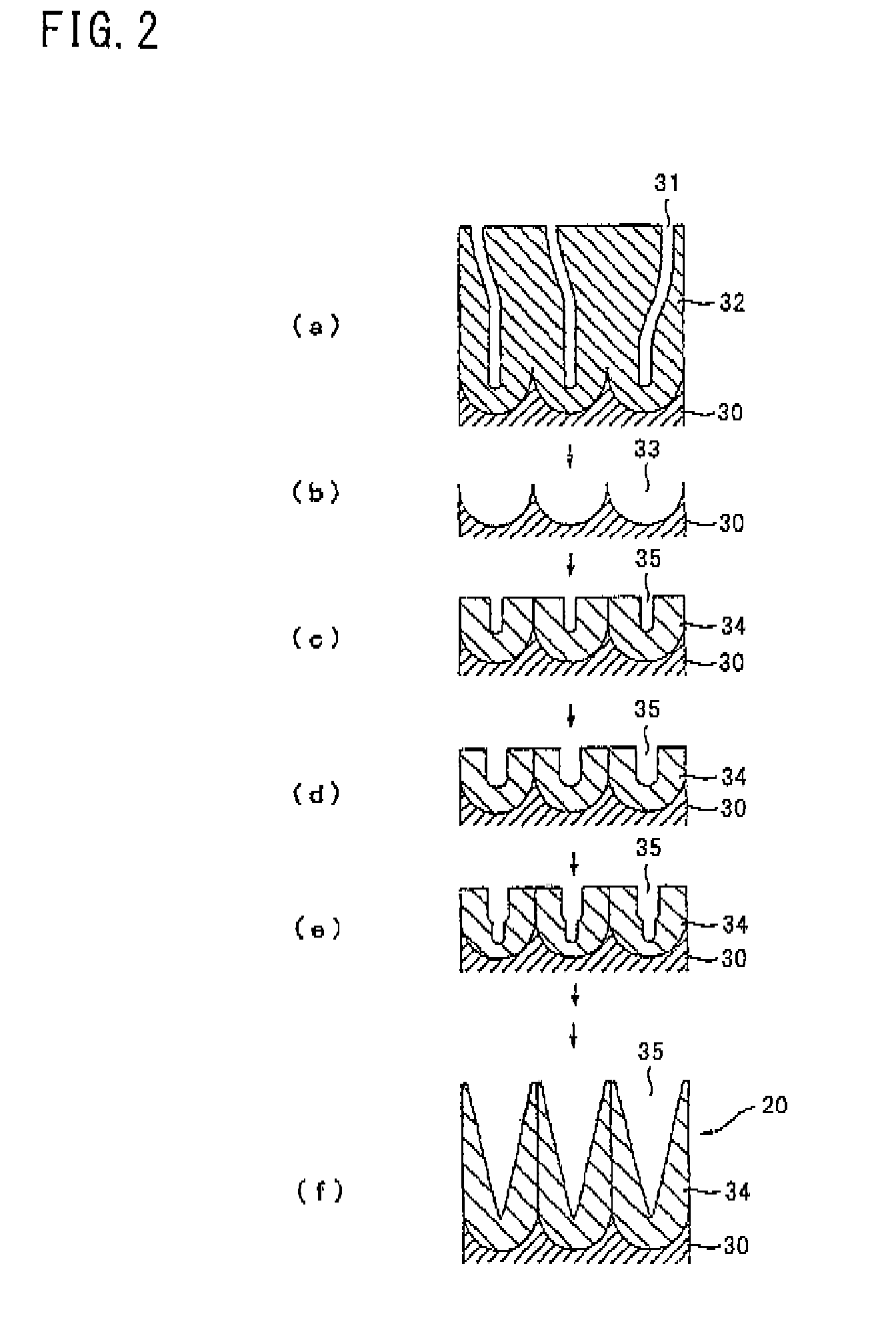
(1) Measurement of Micropores of Stamper:

[0129]Platinum was vapor-deposited on a part of a vertical cross-section of a stamper made of anodized porous alumina for 1 minute. The vertical cross-section was observed using a field emission-type scanning electron microscope (manufactured by JEOL Ltd., trade name: JSM-7400F) at an accelerating voltage of 3.00 kV, whereby intervals (periods) between the adjacent micropores and the depth of the micropores were measured. Specifically, each of the measurements was performed for 10 spots, and the average value thereof was determined as a measured value.

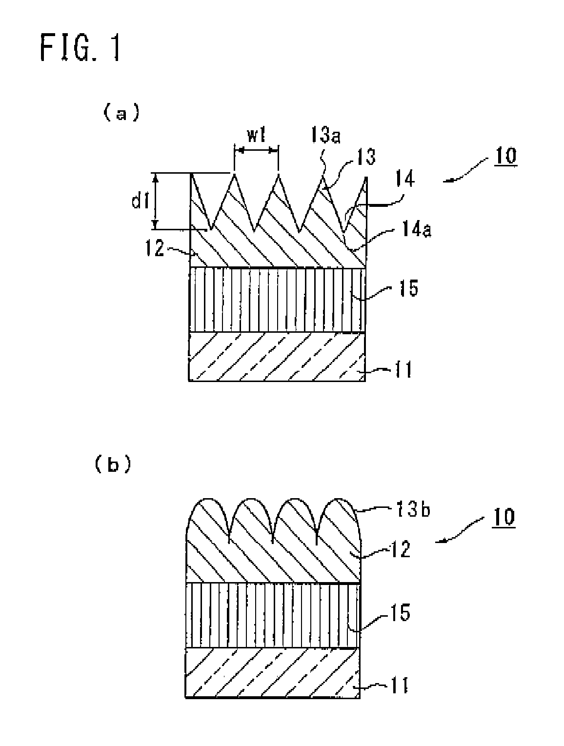
(2) Measurement of Unevenness of Nano Uneven Structure:

[0130]Platinum was vapor-deposited on a ve...

example a1

Formation of Intermediate Layer

[0159]A polyethylene terephthalate film (manufactured by Toyobo Co., Ltd., trade name: A-4300, and thickness: 188 μm) was provided as a transparent substrate. An intermediate layer raw material A1 was uniformly applied on the substrate film using a bar coater, and was left at rest in a drier at 80° C. for 5 minutes. Subsequently, ultraviolet ray was irradiated with energy of 800 mJ / cm2 using a high pressure mercury lamp from the application side of the intermediate layer raw material, to cure a coating, thereby forming an intermediate layer. The thickness of the intermediate layer was 18 μm.

(Formation of Surface Layer Having Nano Uneven Structure)

[0160]A resin composition for forming a surface layer was cast onto a micropore surface of a stamper, and was covered with the substrate film while the substrate film was broadened so that the intermediate layer was brought into contact with the resin composition. Ultraviolet ray was irradiated with energy of ...

examples a2 to a11

and A15 to A17, Comparative Examples A1 to A10, Reference Examples A1 and A2

[0162]Laminates were produced, which had a nano uneven structure having the same size as that of Example A1 on the surface except that intermediate layer raw materials and layer thicknesses shown in Table 2 were employed. The evaluation results are shown in Table 2.

[0163]

TABLE 2Film thicknessFilm thicknessFilmIntermediate layerof intermediateof surfacethicknessPencilScratchraw materiallayer (μm)layer (μm)ratiohardnesstestExample A1Intermediate layer18201.113Hveryraw material 1goodExample A2Intermediate layer18201.113Hveryraw material 2goodExample A3Intermediate layer12141.173Hveryraw material 3goodExample A4Intermediate layer20160.803Hveryraw material 4goodExample A5Intermediate layer8121.503Hgoodraw material 5Example A6Intermediate layer16181.133Hveryraw material 6goodExample A7Intermediate layer16161.003Hveryraw material 7goodExample A8Intermediate layer18160.893Hveryraw material 8goodExample A9Intermediat...


PUM

PropertyMeasurementUnit
thicknessaaaaaaaaaa
vibration frequencyaaaaaaaaaa
compression ratioaaaaaaaaaa

Abstract

A laminate includes a substrate, and a surface layer laminated on the substrate with an intermediate layer sandwiched therebetween. The intermediate layer has a thickness of 8 to 40 μm. The surface layer has a thickness 0.4 to 1.5 times that of the intermediate layer. The laminate satisfies the following (A) and / or (B): (A) tan δ (loss tangent) of the intermediate layer as measured under a condition of a vibration frequency of 1 Hz at 20° C. is 0.2 or greater; and (B) A ratio (MG / SG) of a storage modulus (MG) of the intermediate layer to a storage modulus (SG) of the surface layer as measured under a condition of a vibration frequency of 1 Hz at 20° C. is 0.003 or greater and 0.14 or less.

Description

TECHNICAL FIELD[0001]The present invention relates to a laminate and a method for manufacturing the same. More particularly, the present invention relates to a laminate having excellent scratch resistance even when the laminate has a nano uneven structure on its surface, for example.BACKGROUND ART[0002]It is known that a nano uneven structure body having a nano uneven structure on its surface exhibits antireflective performance according to a change in a continuous refractive index. The nano uneven structure body can also exhibit super-water-repellent performance according to a lotus effect. However, the surface of the nano uneven structure has a nanoscale projecting part which is apt to be inclined, and has lower scratch resistance and durability than a smooth surface made of the same resin.[0003]The following methods are proposed as a method for forming the nano uneven structure: for example, a method for performing injection molding and press molding using a stamper having a reve...

Claims


Application Information

Patent Timeline
Patent Type & Authority Patents(United States)
IPC IPC(8): B32B7/02C09D5/00G02B1/118B05D5/00C08J7/04C08J7/043C08J7/044C08J7/046
CPCC09D5/006B05D5/00C08J7/042G02B1/118C08J2367/02C08J2475/16Y10T428/24355Y10T428/24975B32B2307/536G02B1/18C08J7/043C08J7/046C08J7/044B32B7/02B32B3/30G02B1/11
Inventor TAKIHARA, TSUYOSHIMORI, SEIICHIROOKAMOTO, EIKO
Owner MITSUBISHI CHEM CORP
Why Eureka
Try Eureka