Semiconductor device with light-blocking layers

a semiconductor and memory element technology, applied in the direction of capacitors, digital storage, instruments, etc., can solve the problems of difficult capacitors, achieve the effects of preventing the leakage of charge from the memory element, preventing the degradation of the characteristics of the transistor due to light, and suppressing the shift of the threshold voltag

Active Publication Date: 2016-03-29
SEMICON ENERGY LAB CO LTD
View PDF223 Cites 6 Cited by
  • Summary
  • Abstract
  • Description
  • Claims
  • Application Information

AI Technical Summary

Benefits of technology

[0004]In the case of a semiconductor memory device in which a transistor including the oxide semiconductor in a channel formation region is used as a switching element (hereinafter simply referred to as a memory device), the threshold voltage of the transistor shifts or off-state current is increased, so that charge to be held in a memory element is easily discharged and a period in which data can be held tends to be shortened. Accordingly, in order to ensure a longer period in which accurate data is held in a memory device, it is important to prevent degradation of characteristics of a transistor due to light irradiation.
[0010]An oxide semiconductor has a band gap approximately three times as large as that of silicon and has the intrinsic carrier density lower than that of silicon. With a channel formation region including a semiconductor material having the above characteristics, a transistor with extremely small off-state current can be realized. The transistor having the above structure is used as a switching element for holding charge accumulated in a memory element, whereby leakage of charge from the memory element can be prevented.
[0011]An oxide semiconductor is a metal oxide having semiconductor characteristics, and has mobility approximately as high as microcrystalline or polycrystalline silicon and uniform element characteristics which is a characteristic of amorphous silicon. An oxide semiconductor highly purified (a purified OS) by reduction in concentration of impurities such as moisture or hydrogen, which serves as electron donors (donors), is an i-type semiconductor (an intrinsic semiconductor) or a substantially i-type semiconductor. Therefore, a transistor including the oxide semiconductor has a characteristic of extremely small off-state current. Specifically, the hydrogen concentration in the highly purified oxide semiconductor which is measured by secondary ion mass spectrometry (SIMS) is less than or equal to 5×10¹⁹ / cm3, preferably less than or equal to 5×10¹⁸ / cm3, more preferably less than or equal to 5×10¹⁷ / cm3, still more preferably less than or equal to 1×10¹⁶ / cm3. In addition, the carrier density of the oxide semiconductor film, which is measured by Hall effect measurement, is less than 1×10¹⁴ / cm3, preferably less than 1×10¹² / cm3, more preferably less than 1×10¹¹ / cm3. Furthermore, the band gap of the oxide semiconductor is 2 eV or more, preferably 2.5 eV or more, more preferably 3 eV or more. With the use of a highly purified oxide semiconductor film with sufficiently reduced concentration of impurities such as moisture or hydrogen, off-state current or leakage current of the transistor can be reduced.
[0016]In one embodiment of the present invention, a transistor in which an oxide semiconductor is included in an active layer is used as a switching element for controlling holding of charge in a memory element, whereby leakage of charge from the memory element can be prevented. Further, the active layer is sandwiched between an electrode and a conductive film or an insulating layer, which have a light-blocking property, so that degradation of characteristics of the transistor due to light can be prevented. Specifically, shifts of the threshold voltage can be suppressed and increase in off-state current can be prevented. Further, in one embodiment of the present invention, the electrode having a light-blocking property is used as an electrode of a capacitor. Therefore, since the capacitor is provided so as to overlap with the transistor in a memory cell, an area occupied by the memory cell can be reduced while an area occupied by the capacitor, or a capacitance value is ensured.
[0017]Accordingly, in a memory device according to one embodiment of the present invention, memory capacity per unit area can be increased while a period in which data is held is ensured. Further, in the present invention, the memory device is used in a semiconductor device, so that the reliability of the semiconductor device can be increased and high functionality can be achieved.

Problems solved by technology

Therefore, it is difficult for a capacitor to ensure a capacitance value enough to hold data for a long time in a memory device.

Method used


Image

  • Semiconductor device with light-blocking layers
  • Semiconductor device with light-blocking layers
  • Semiconductor device with light-blocking layers

Examples


embodiment 1

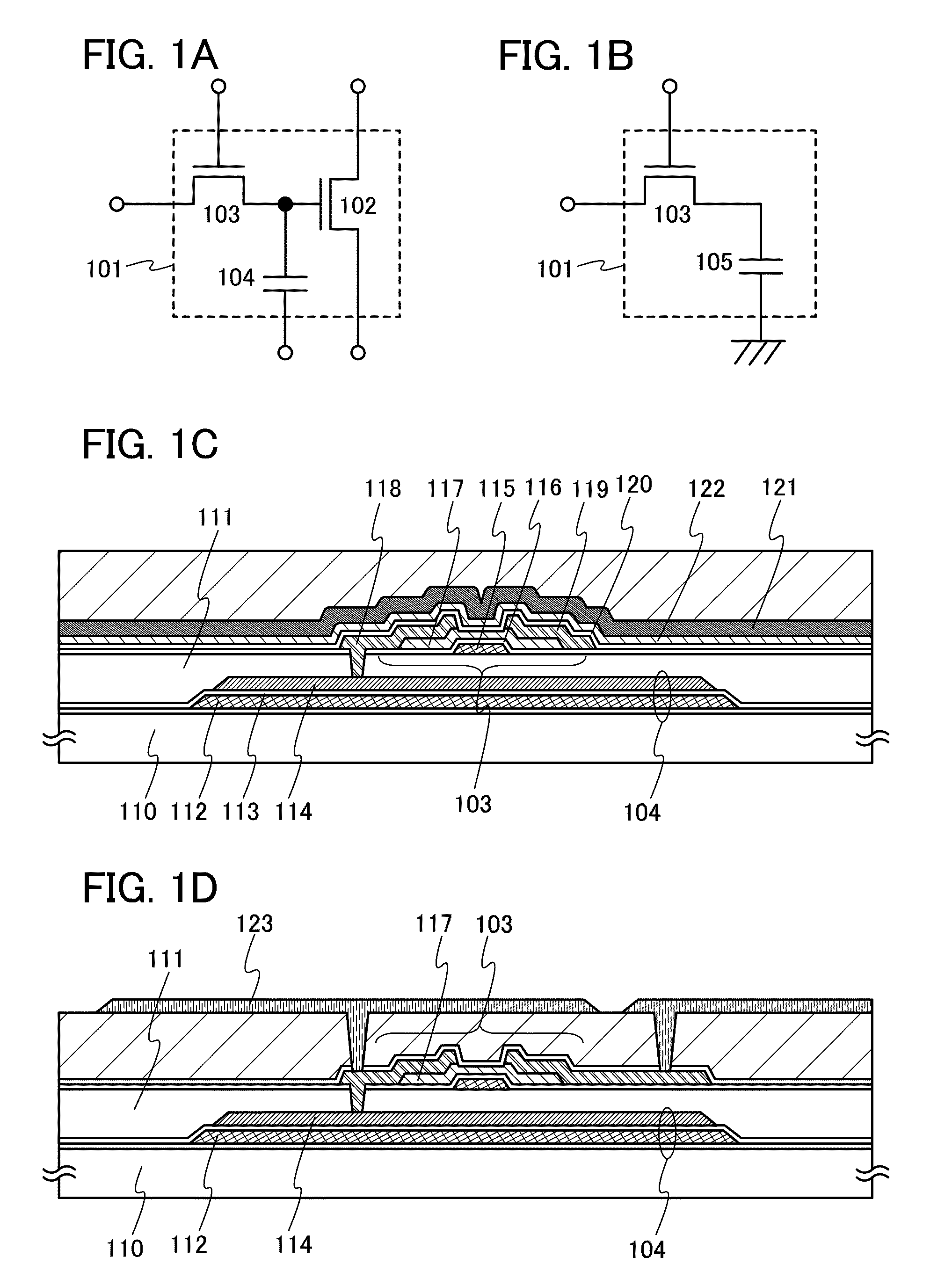
[0040]FIG. 1A illustrates a circuit diagram of a structure of a memory cell in a memory device according to one embodiment of the present invention, as an example. In the circuit diagram illustrated in FIG. 1A, a memory cell 101 includes a transistor 102 serving as a memory element, a transistor 103 serving as a switching element, and a capacitor 104. In the transistor 102 serving as a memory element, charge is accumulated in a gate capacitor formed between a gate electrode and an active layer, whereby data is stored.

[0041]Note that the memory cell 101 may further include another circuit element such as a transistor, a diode, a resistor, a capacitor, or an inductor as needed.

[0042]The terms of the “source electrode” and the “drain electrode” included in the transistor interchange with each other depending on the polarity of the transistor or difference between the levels of potentials applied to the respective electrodes. In general, in an n-channel transistor, an electrode to which...

embodiment 2

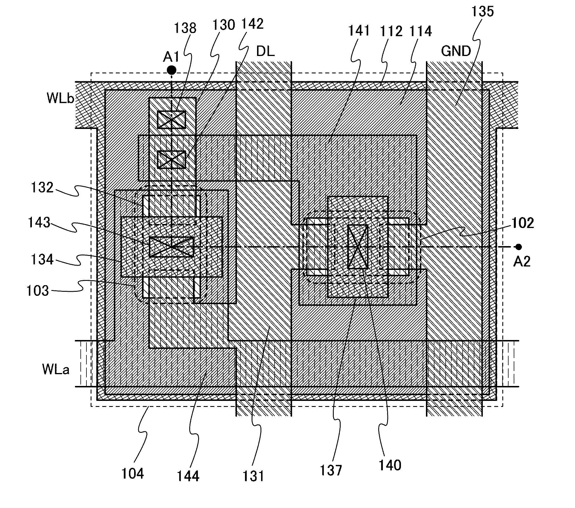
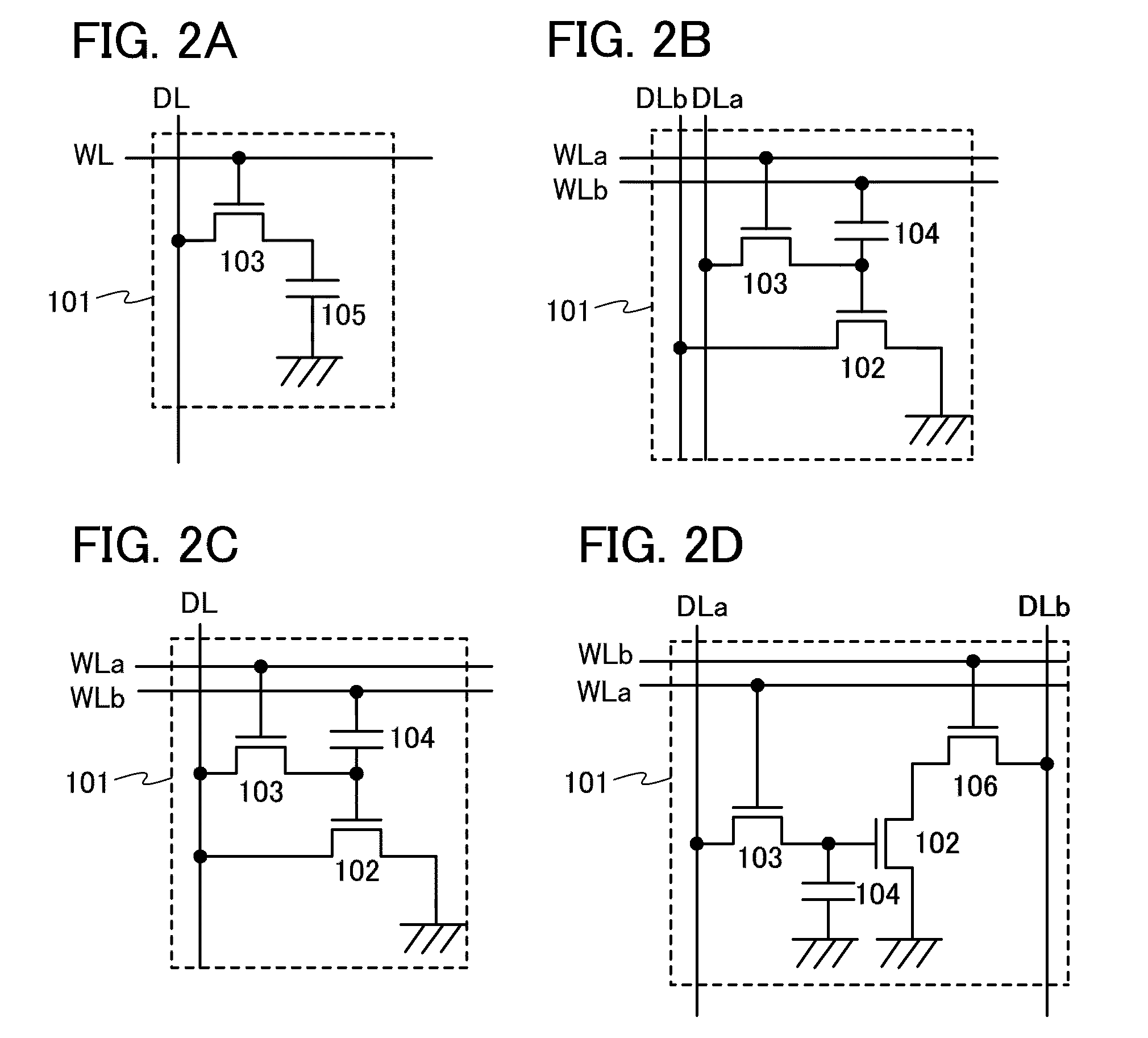
[0095]In this embodiment, one example of a specific structure of a memory cell included in a memory device according to one embodiment of the present invention will be described. Note that in this embodiment, the structure of the memory cell having the circuit structure illustrated in FIG. 2C will be described as an example.

[0096]FIG. 3 is an example of a top view of the memory cell. Note that in FIG. 3, an insulating film other than a light-blocking insulating film is omitted in order to clarify the structure of the memory cell. A cross-sectional view taken along dotted line A1-A2 in FIG. 3 is illustrated in FIG. 4.

[0097]The memory cell illustrated in FIG. 3 and FIG. 4 includes, over the substrate 110 having an insulating surface, the transistor 102, the transistor 103, and the capacitor 104. The capacitor 104 formed over the substrate 110 is covered with the insulating film 111 and the transistor 102 and the transistor 103 are formed over the insulating film 111. The capacitor 104...

embodiment 3

[0134]In this embodiment, an example of a structure of the transistor 103 serving as a switching element, which is different from the structure illustrated in FIG. 1D, will be described.

[0135]An example of a cross-sectional view of the transistor 103 and the capacitor 104 is illustrated in FIG. 5A. Although FIG. 5A illustrates a cross-sectional structure of the memory cell 101 illustrated in FIG. 1A, the transistor 103 and the capacitor 105 in FIG. 1B can have structures similar to those illustrated in FIG. 5A.

[0136]In the cross-sectional view illustrated in FIG. 5A, as in FIG. 1D, the capacitor 104 and the transistor 103 are formed over the substrate 110 having an insulating surface, and the capacitor 104 and the transistor 103 overlap with each other with the insulating film 111 interposed therebetween.

[0137]A specific structure of the capacitor 104 is the same as that illustrated in FIG. 1D. FIG. 5A is different from FIG. 1D in that the transistor 103 has a channel protective str...


PUM


Abstract

One object is to propose a memory device in which a period in which data is held can be ensured and memory capacity per unit area can be increased. The memory device includes a memory element, a transistor including an oxide semiconductor in an active layer for control of accumulating, holding, and discharging charge in the memory element, and a capacitor connected to the memory element. At least one of a pair of electrodes of the capacitor has a light-blocking property. Further, the memory device includes a light-blocking conductive film or a light-blocking insulating film. The active layer is positioned between the electrode having a light-blocking property and the light-blocking conductive film or the light-blocking insulating film.

Description

TECHNICAL FIELD[0001]The present invention relates to a memory device and a semiconductor device including the memory device.BACKGROUND ART[0002]In recent years, a metal oxide having semiconductor characteristics, which is called an oxide semiconductor, has attracted attention as a novel semiconductor material having high mobility as in the case of polysilicon or microcrystalline silicon and having uniform element characteristics as in the case of amorphous silicon. A metal oxide is used for various applications. For example, indium oxide is a well-known metal oxide and used as a material of a transparent electrode included in a liquid crystal display device or the like. Examples of such metal oxides having semiconductor characteristics include tungsten oxide, tin oxide, indium oxide, and zinc oxide. Insulated-gate field-effect transistors (hereinafter simply referred to as transistors) in each of which such metal oxide having semiconductor characteristics is used for a channel form...

Claims


Application Information

Patent Timeline
Patent Type & Authority Patents(United States)
IPC IPC(8): H01L29/04G11C7/02G11C5/00H01L27/12G11C11/404H01L49/02H01L27/115H01L27/108G11C16/34G11C16/18G11C16/04
CPCH01L27/1225G11C5/005G11C7/02G11C11/404H01L27/10873H01L27/1156H01L27/11517H01L27/1255H01L28/60G11C16/0433G11C16/18G11C16/349H10B12/05H10B41/00H10B41/70
Inventor SAITO, TOSHIHIKO
Owner SEMICON ENERGY LAB CO LTD
Why Eureka
Try Eureka