Modulation circuit and semiconductor device including the same

a technology of modulation circuit and semiconductor device, which is applied in the direction of modulation, semiconductor/solid-state device details, instruments, etc., can solve the problems of reducing the reliability of rfid communication and increasing power consumption, so as to reduce the power consumption of the modulation circuit, and reduce the power consumption

Active Publication Date: 2016-05-24
SEMICON ENERGY LAB CO LTD
View PDF150 Cites 9 Cited by
  • Summary
  • Abstract
  • Description
  • Claims
  • Application Information

AI Technical Summary

Benefits of technology

[0008]A modulation circuit that employs a load modulation method includes a switching element and a load. A transistor whose channel formation region is formed using silicon is used as the switching element. However, in a transistor whose channel formation region is formed using silicon, off-state current (also referred to as leakage current) which occurs when the transistor is in the off state is high, which increases power consumption. This results in a reduction in the reliability of RFID communication.
[0009]In view of the above problem, an object of one embodiment of the present invention is to reduce the power consumption of a modulation circuit. Another object of one embodiment of the present invention is to reduce the power consumption of a semiconductor device having a modulation circuit by reducing the power consumption of the modulation circuit. Another object of one embodiment of the present invention is to increase the maximum communication distance of an RF tag having a modulation circuit by reducing the power consumption of the RF tag having a modulation circuit. Another object of one embodiment of the present invention is to improve the response reliability of the RF tag.
[0026]One embodiment of the present invention can reduce the power consumption of a modulation circuit. Reducing the power consumption of the modulation circuit can reduce the power consumption of a semiconductor device having the modulation circuit. Reducing the power consumption of an RF tag having a modulation circuit can increase the maximum communication distance of the RF tag. In addition, one embodiment of the present invention can achieve improvement in the reliability of a semiconductor device having a modulation circuit.

Problems solved by technology

However, in a transistor whose channel formation region is formed using silicon, off-state current (also referred to as leakage current) which occurs when the transistor is in the off state is high, which increases power consumption.
This results in a reduction in the reliability of RFID communication.

Method used


Image

  • Modulation circuit and semiconductor device including the same
  • Modulation circuit and semiconductor device including the same
  • Modulation circuit and semiconductor device including the same

Examples


embodiment 1

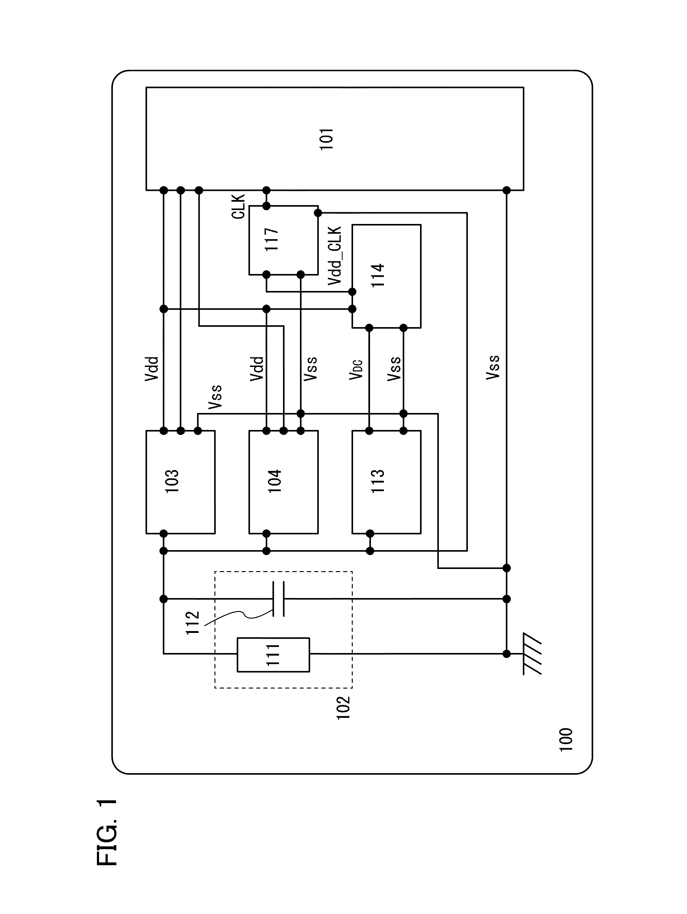
[0051]FIG. 1 shows the block diagram of the whole RF tag which is used as one embodiment of the present invention. An RF tag 100 include: a logic circuit 101 which carries out functional processing, e.g. generates a response signal in response to data received; an antenna circuit 102 which sends and receives signals to / from (communicates with) a reader / writer; a demodulation circuit 103 which demodulates an amplitude-modulated wave (obtained by superimposing a modulated wave on a carrier wave) received by the antenna circuit 102 to extract a pulsed signal; a modulation circuit 104 which modulates a carrier wave outputted from the reader / writer in response to a response signal outputted from the logic circuit 101 and transmitting a response signal to the reader / writer; a rectifier circuit 113 for generating a DC voltage from a carrier wave or amplitude-modulated wave received by the antenna circuit 102; a constant-voltage circuit 114 which converts DC voltage generated by the rectifi...

embodiment 2

[0060]In this embodiment, the configuration of the modulation circuit described in Embodiment 1 will be described.

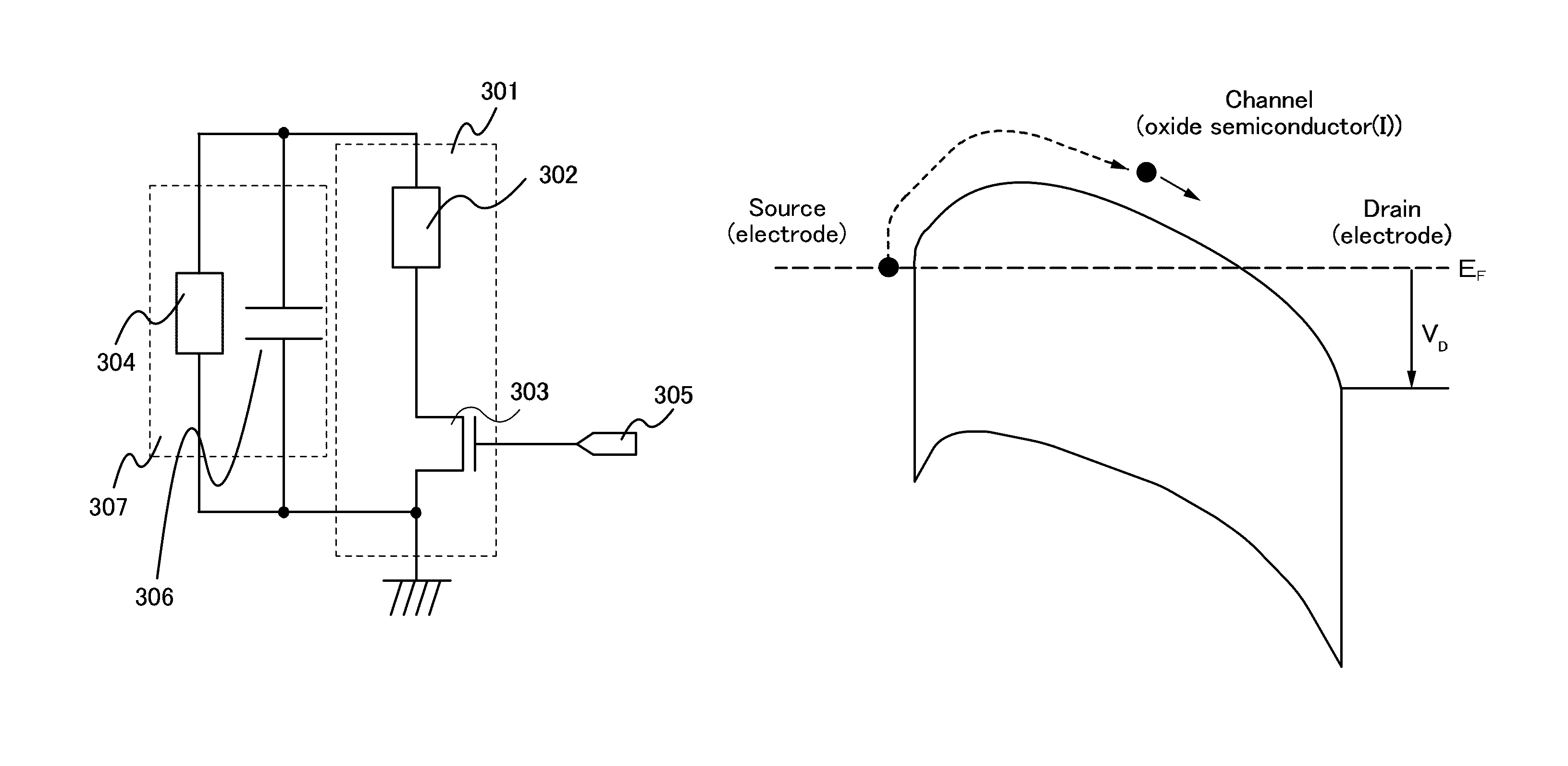
[0061]FIG. 3 shows an example of the circuit configuration of the modulation circuit according to one embodiment of the present invention. A modulation circuit 301 employs a load modulation method, and includes a load 302 and a transistor 303. One of the source and drain of the transistor 303 is electrically connected to one terminal of an antenna 304 through the load 302. The other of the source and drain is electrically connected to the other terminal of the antenna 304. The on / off of the transistor 303 is controlled in accordance with a signal 305 inputted to the gate of the transistor 303. Note that the signal 305 inputted to the gate of the transistor 303 is a binary signal with high (H) or low (L), and corresponds to a response signal outputted from the logic circuit (also referred to as a subcarrier).

[0062]In this manner, the modulation circuit 301 using a load mo...

embodiment 3

[0105]In this embodiment, a configuration whereby the power consumption of the modulation circuit is further reduced will be described.

[0106]First, one example of the configuration of the modulation circuit of this embodiment will be described with reference to FIG. 7. FIG. 7 is different from FIG. 3 described in Embodiment 1 in that a modulation circuit 701 shown in FIG. 7 has a load 702, a transistor 703, and a diode 720 which are connected in series between the two terminals of the antenna 304, while the modulation circuit 301 shown in FIG. 3 has the load 302 and the transistor 303 are connected in series between the two terminals of the antenna 304. In other words, the modulation circuit 701 shown in FIG. 7 includes the load 702, the transistor 703, and the diode 720. One terminal of the load 702 is electrically connected to one terminal of the antenna 304, and the other terminal of the load 702 is electrically connected to the anode (one terminal) of the diode 720. The cathode ...


PUM


Abstract

A modulation circuit includes a load and a transistor serving as a switch. The transistor has an oxide semiconductor layer in which hydrogen concentration is 5×10¹⁹ / cm3 or less. The off-state current of the transistor is 1×10⁻¹³ A or less. A modulation circuit includes a load, a transistor serving as a switch, and a diode. The load, the transistor, and the diode are connected in series between the terminals of an antenna. The transistor has an oxide semiconductor layer in which hydrogen concentration is 5×10¹⁹ / cm3 or less. An off-state current of the transistor is 1×10⁻¹³ A or less. On / off of the transistor is controlled in accordance with a signal inputted to a gate of the transistor. The load is a resistor, a capacitor, or a combination of a resistor and a capacitor.

Description

BACKGROUND OF THE INVENTION[0001]1. Field of the Invention[0002]The present invention relates to a semiconductor device, particularly to a modulation circuit. Further, the present invention relates to a semiconductor device (a data carrier) capable of wirelessly communicating (transmitting and receiving) data.[0003]2. Description of the Related Art[0004]In recent years, individual identification technologies have attracted attention. In these technologies, an ID number (an identification number) is assigned to each individual object, thereby revealing the information history of individual objects. These technologies are utilized for production, management, or the like. In particular, RFID (radio frequency identification) technologies used for sending and receiving data by wireless communication are spreading. A wireless communication system using RFID technologies includes a radio communication device (an interrogator) and a data carrier (a responder), and data is wirelessly transfe...

Claims


Application Information

Patent Timeline
Patent Type & Authority Patents(United States)
IPC IPC(8): H01L29/786H03C1/36
CPCH03C1/36H01L29/78693H01L28/20H01L28/40G06K19/07775H01L23/66H01L27/0629H01L29/7869H01L29/78696H01L2223/6677H04M2201/04H04M2201/06
Inventor KAMATA, KOICHIRO
Owner SEMICON ENERGY LAB CO LTD
Why Eureka
Try Eureka