Apparatus and method for a high precision voltage reference
a voltage reference circuit, high-precision technology, applied in the direction of electrical variable regulation, process and machine control, instruments, etc., can solve the problems of high cost, physical size of transistors, number of transistors, etc., and achieve the effect of less cos
- Summary
- Abstract
- Description
- Claims
- Application Information
AI Technical Summary
Benefits of technology
Problems solved by technology
Method used
Image

Examples
embodiment 300
[0039]FIG. 3 is a circuit schematic of a voltage reference circuit 300 in accordance with a further embodiment of the disclosure. In some cases, the gain of loop on A1330-N3325-N2320 might be too large in magnitude in order to get enough phase margin. Then the loop gain could be decreased by putting a resistor between the source of the n-channel MOS N3325 and the ground 302. The embodiment 300 comprises a VDD 301 and ground VSS 302. A current mirror is formed with transistor N1310 and transistor N2320. Differential inputs for amplifier A1330 are input 327 and input 329 connected to the drain of the N1310, and N2320. A second current mirror is formed with p-channel MOSFET P1340, P2345, and P3350. The current source 303 establishes a current Is and is connected to the p-channel MOSFET current mirror. The amplifier A1330 provides a feedback signal 335 to n-channel MOSFET N3325. The drain of N3325 is coupled to output O 337 and whose source is connected to resistor R 355.
embodiment 400
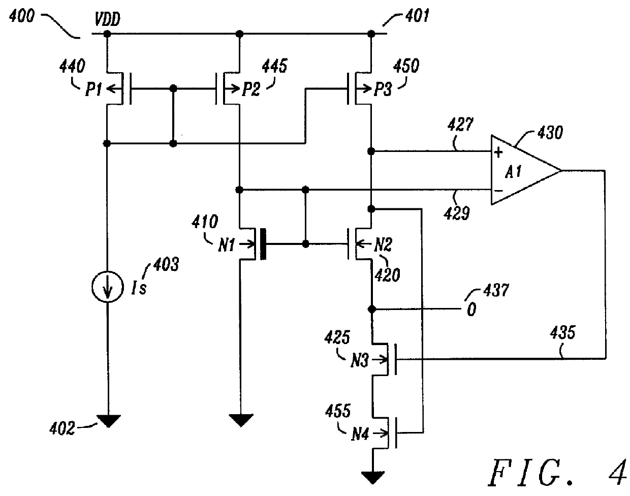
[0040]FIG. 4 is a circuit schematic of a voltage reference circuit 400 in accordance with another embodiment of the disclosure. This is another method to decrease the loop gain. The embodiment 400 comprises a VDD 401 and ground VSS 402. A current mirror is formed with transistor N1410 and transistor N2420. Differential inputs for amplifier A1430 are input 427 and input 429 connected to the drain of the N1410, and N2420. The drain of N2420 is coupled to the gate of n-channel MOSFET N4455. A second current mirror is formed with p-channel MOSFET P1440, P2445, and P3450. The current source 403 establishes a current Is and is connected to the p-channel MOSFET current mirror. The amplifier A1430 provides a feedback signal 435 to n-channel MOSFET N3425. The drain of N3425 is coupled to output O 437. In this circuit, the n-channel MOSFET device N4455 is added instead of the resistor R 355 of FIG. 3. The resistor R 355 of FIG. 3 might need a large area due to the magnitude of the resistor va...
embodiment 500
[0041]FIG. 5 is a circuit schematic of a voltage reference circuit 500 in accordance with another embodiment of the disclosure. Another method to decrease the loop gain is achieved with this circuit embodiment. The embodiment 500 comprises a VDD 501 and ground VSS 502. A current mirror is formed with transistor N1510 and transistor N2520. Differential inputs for amplifier A1530 are input 527 and input 529 connected to the drain of the N1510, and N2520. A second current mirror is formed with p-channel MOSFET P1540, P2545, and P3550. The current source 503 establishes a current Is and is connected to the p-channel MOSFET current mirror. The amplifier A1530 provides a feedback signal 535 to p-channel MOSFET P4525. If the threshold voltage of the p-channel MOS P4525 is low, it doesn't affect the voltage of output O 537, and as a result, this circuit will have good output accuracy and good stability (e.g. because of lowest loop gain).
[0042]FIG. 6 is a circuit schematic of a voltage refer...
PUM
 Abstract
Description
Claims
Application Information
 - R&D
- Intellectual Property
- Life Sciences
- Materials
- Tech Scout
- Unparalleled Data Quality
- Higher Quality Content
- 60% Fewer Hallucinations
Browse by: Latest US Patents, China's latest patents, Technical Efficacy Thesaurus, Application Domain, Technology Topic, Popular Technical Reports.
© 2025 PatSnap. All rights reserved.Legal|Privacy policy|Modern Slavery Act Transparency Statement|Sitemap|About US| Contact US: help@patsnap.com