
Touch panel and display device

a display device and touch panel technology, applied in the field of touch panel and display device, can solve the problems of changing the resistance value of the first electrode layer or the second electrode layer, the oca does not stick, and the gap is developed, so as to improve the image quality of the touch panel, reduce the widthwise dimension, and reduce the cell pitch

Active Publication Date: 2016-07-19
FUJIFILM CORP
View PDF8 Cites 2 Cited by
  • Summary
  • Abstract
  • Description
  • Claims
  • Application Information

AI Technical Summary

Benefits of technology

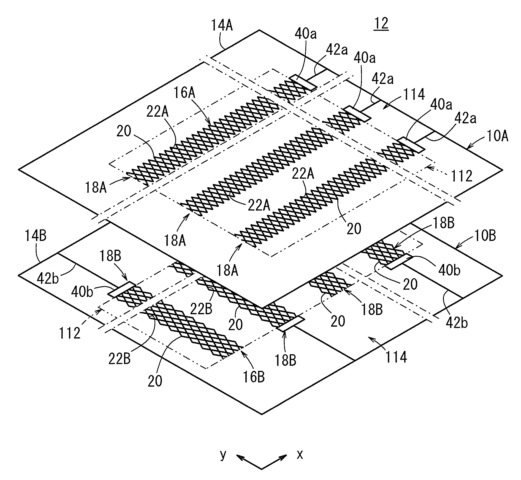
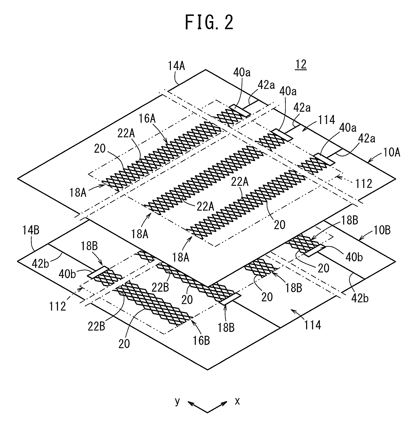
[0006]On the condition that the silver mesh transparent electrodes, as disclosed in Japanese Laid-Open Patent Publication No. 2011-517355 (PCT), are used in a touch panel, then the silver mesh transparent electrodes are effective to reduce the cell pitch, reduce the widthwise dimension of the fine silver lines, and arrange the fine silver lines obliquely to the layout of pixels of a liquid crystal display or the like, such that each cell is of a lozenge shape or a parallelogrammatic shape having acute angles, in order to improve the touch panel in terms of image quality based on increased mesh visibility and transmittance, as well as to achieve a reduction in moire phenomena.
[0008]As a consequence, water is likely to find its way through the gaps in the acute-angled portions, causing ion migration, which leads to faults such as a change in the resistance value of the first electrode layer or the second electrode layer, as well as short circuiting. It has been found that faults due to ion migration are liable to happen on condition that the widthwise dimension of the fine silver lines is reduced as much as possible, e.g., to 4 μm or less, in recent attempts to increase the visibility of the touch panel.
[0009]A major object of the present invention is to provide a touch panel, which employs an OCA that is capable of seeping suitably into the acute-angled portions of cells, to thereby prevent the fine silver lines from suffering from ion migration.
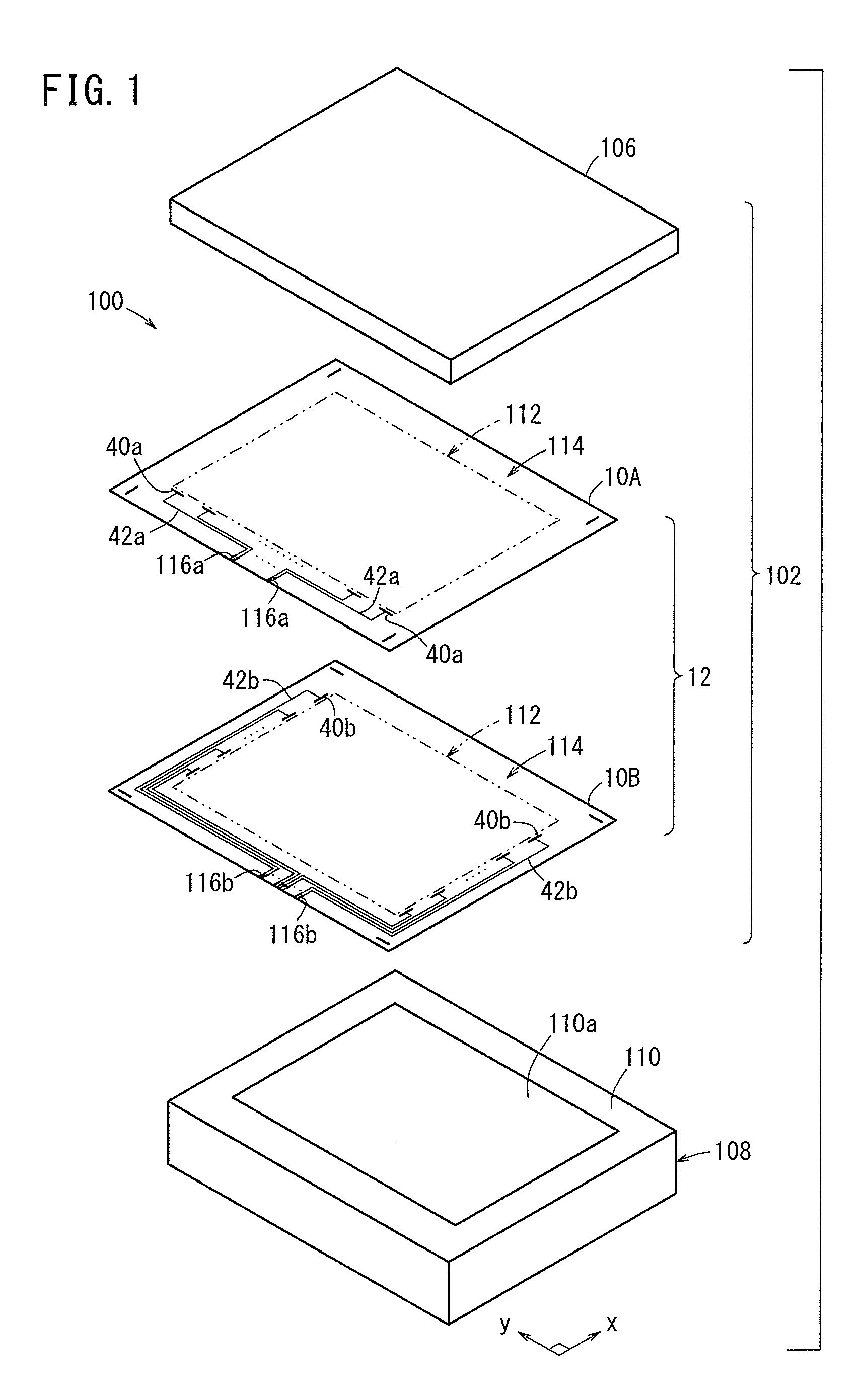
[0019]The touch panel employs an adhesive (OCA) having prescribed properties. Since the OCA exhibits an excellent ability of seeping into acute-angled portions, and suitably covers the electrodes where the cells are of a parallelogrammatic shape having acute angles, gaps are unlikely to be formed between the electrodes and the OCA. Therefore, entry of water between the electrodes and the OCA is avoided. Thus, the silver of the fine silver lines is prevented from suffering from ion migration.
[0020]On the condition that the fine silver lines, whose visibility is particularly excellent, have a widthwise dimension of 2 μm or less, then the resistance value of the fine silver lines (electrodes) tends to change significantly due to ion migration. According to the present invention, which uses the OCA, even though the electrodes are made up of very fine lines, the resistance value of the electrodes is prevented from changing.
[0032]Since the touch panel according to the present invention uses the aforementioned adhesive, which exhibits prescribed properties, the silver of the fine silver lines, which function as electrodes with excellent visibility, is prevented from suffering from ion migration, and the resistance value of the electrodes is prevented from changing. Thus, the touch panel exhibits excellent visibility.

Problems solved by technology

However, in a case where an OCA is applied to a silver mesh transparent electroconductive film, which includes cells of a lozenge shape or a parallelogrammatic shape having acute angles, the OCA fails to enter into the acute-angled portions of the cells, i.e., a seepage failure occurs, resulting in a problem in that the OCA does not stick to the acute-angled portions, but gaps are developed therein.
As a consequence, water is likely to find its way through the gaps in the acute-angled portions, causing ion migration, which leads to faults such as a change in the resistance value of the first electrode layer or the second electrode layer, as well as short circuiting.
It has been found that faults due to ion migration are liable to happen on condition that the widthwise dimension of the fine silver lines is reduced as much as possible, e.g., to 4 μm or less, in recent attempts to increase the visibility of the touch panel.

Method used


Image

  • Touch panel and display device
  • Touch panel and display device
  • Touch panel and display device

Examples


##ventive example 1

Inventive Example 1

[0150]Inventive examples of the present invention will be described below in specific detail. The materials, amounts used, ratios, processing details, and processing sequences described in the inventive examples can be changed without departing from the spirit of the present invention. Therefore, the scope of the present invention shall not be interpreted as being restricted by the specific examples described below.

[OCA]

[0151]According to Table 1, principal components and 0.04 parts by weight of IRGACURE 651 (trademark of 2,2-dimethoxy-2-phenylacetophenon manufactured by Ciba Japan, hereinafter referred to as “Irg651”) as a photopolymerization initiator were weighed and mixed together suitably in a glass container, and a nitrogen gas was substituted for dissolved oxygen, after which the solution was irradiated with ultraviolet rays for several minutes by a low-pressure mercury lamp in order to bring about partial polymerization, thereby obtaining a viscous liquid ...


PUM


Abstract

A touch panel and a display device are disclosed. Either a cell or a cell, which is formed by the intersections of silver fine wires which form either first electrodes or second electrodes, forms parallelogram shapes (preferably rhomboids), having opposite angles wherein intersection angles are obtuse angles and intersection angles are acute angles. The first electrodes and / or the second electrodes have an adhesive (OCA) deployed thereupon, which has a loss coefficient (tan δ) of 0.13 or more at 140° C. and 1 Hz, and a reserve elasticity of 8.9×10⁴ Pa or less at 25° C. and 1 Hz.

Description

CROSS-REFERENCE TO RELATED APPLICATIONS AND PRIORITY CLAIMS[0001]This application is a Continuation of International Application No. PCT / JP2014 / 053585 filed on Feb. 17, 2014, which was published under PCT Article 21(2) in Japanese, which is based upon and claims the benefit of priority from Japanese Patent Application No. 2013-064316 filed on Mar. 26, 2013, the contents all of which are incorporated herein by reference.TECHNICAL FIELD[0002]The present invention relates to a touch panel and a display device, and more particularly to a touch panel and a display device that are provided with cells of a parallelogrammatic shape, which are defined by fine lines of silver crossing each other.BACKGROUND ART[0003]Touch panels are provided with sensors that detect the position where the touch panel surface is pressed by an object (e.g., a finger). Each of such sensors includes first electrodes and second electrodes, which extend perpendicularly to each other. As is well known in the art, an ...

Claims


Application Information

Patent Timeline
Patent Type & Authority Patents(United States)
IPC IPC(8): G09G5/00G06F3/047G06F3/041G06F3/044
CPCG06F3/047G06F3/041G06F3/044G06F3/0412G06F2203/04103G06F2203/04112G06F3/0445G06F3/0446
Inventor NAKAYAMA, MASAYAHASEGAWA, KAZUHIRO
Owner FUJIFILM CORP
Learn More