Lateral-diffusion metal-oxide-semiconductor device

a metal-oxide-semiconductor and lateral technology, applied in semiconductor devices, semiconductor/solid-state device details, electrical apparatus, etc., can solve the problems of reducing ron and applicability of ldmos devices, and achieves reducing cell pitch, reducing ron, and improving breakdown voltage

Active Publication Date: 2013-05-28
UNITED MICROELECTRONICS CORP
View PDF5 Cites 3 Cited by
  • Summary
  • Abstract
  • Description
  • Claims
  • Application Information

AI Technical Summary

Benefits of technology

[0010]According to the LDMOS transistor device, the common source having an optimal layout pattern is provided to reduce the cell pitch and the doped regions of the drain that provided surrounding the gate are used to reduce the Ron and simultaneously improve the breakdown voltage.

Problems solved by technology

Furthermore, such limitations is not only adverse to reduce the Ron but also adverse to the applicability of the LDMOS device 100.

Method used


Image

  • Lateral-diffusion metal-oxide-semiconductor device
  • Lateral-diffusion metal-oxide-semiconductor device
  • Lateral-diffusion metal-oxide-semiconductor device

Examples


Embodiment Construction

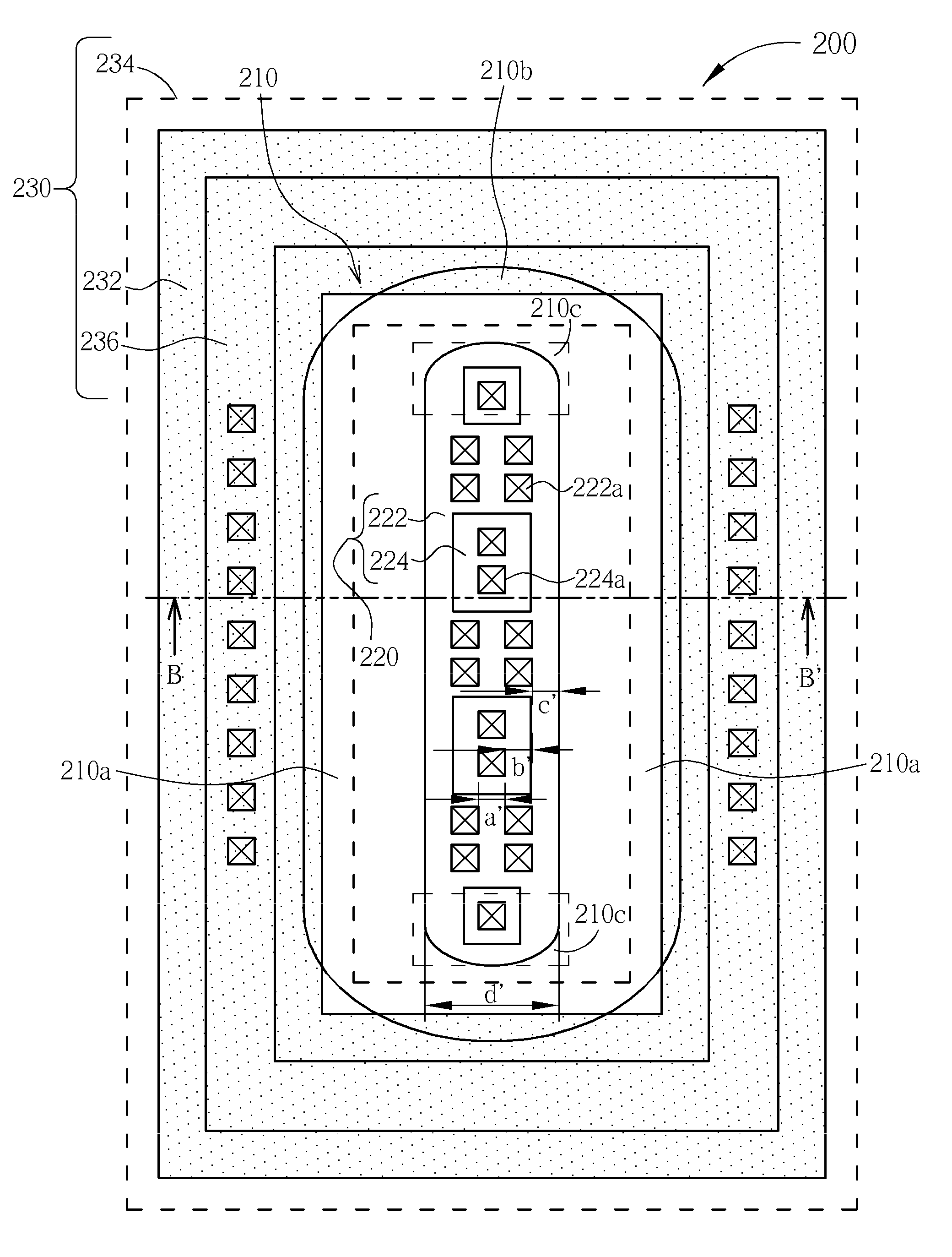
[0018]Please refer to FIGS. 4-6, FIG. 4 is a schematic drawing illustrating a LDMOS device provided by a preferred embodiment of the present invention, FIG. 5 is a cross-sectional view taken along a crossing line B-B′ in FIG. 4, and FIG. 6 is a schematic drawing illustrating a modification to the LDMOS device of the preferred embodiment. As shown in FIGS. 4-5, the LDMOS device 200 provided by the preferred embodiment includes a semiconductor substrate 202, which has a first conductive type, and a deep well region 204 having a second conductive type formed therein. In the preferred embodiment, the first conductive type is P-type and the second conductive type is N-type. However, those skilled in the art would easily realize that it is not limited to have the first conductive type being N-type and the second conductive type being P-type. Accordingly, the LDMOS device 200 provided by the preferred embodiment is a P-type LDMOS device positioned on an N-type deep well region 204 in a P-t...


PUM


Abstract

A lateral-diffusion metal-oxide-semiconductor device includes a semiconductor substrate having at least a field oxide layer, a gate having a layout pattern of a racetrack shape formed on the substrate, a common source formed in the semiconductor substrate and enclosed by the gate, and a drain surrounding the gate and formed in the semiconductor substrate. The gate covers a portion of the field oxide layer. The common source includes a first doped region having a first conductive type and a plurality of islanding second doped regions having a second conductive type. The drain includes a third doped region having the first conductive type. The third doped region overlaps a portion of the field oxide layer and having an overlapping area between the third doped region and the field oxide layer.

Description

BACKGROUND OF THE INVENTION[0001]1. Field of the Invention[0002]The present invention relates generally to a lateral-diffusion metal-oxide-semiconductor (LDMOS) device, and more particularly, to a LDMOS device having low On-state resistance (Ron).[0003]2. Description of the Prior Art[0004]With the progress of semiconductor integrated circuits manufacturing, it is more preferable to have controllers, memories, devices for low-voltage operation and power devices for high-voltage operation integrated in one single-chip system. Therefore the prior art has employed the insulated gate bipolar transistor (IGBT) and double-diffused metal oxide semiconductor (DMOS) transistor devices as the power devices of high-voltage operation in the single-chip system.[0005]The DMOS transistor device can be categorized into the lateral DMOS (LDMOS) device and the vertical DMOS (VDMOS) device. Having advantage of higher operational bandwidth, higher operational efficiency, and convenience to be integrated...

Claims


Application Information

Patent Timeline
Patent Type & Authority Patents(United States)
IPC IPC(8): H01L23/62
CPCH01L29/0692H01L29/4238H01L29/7835H01L29/0847H01L29/41758H01L29/42368H01L29/0878
Inventor LIN, HONG-ZEHUANG, BO-JUICHEN, CHIN-LUNGYAN, TING-ZHOULIAO, WEI-SHANHUANG, HAN-MINLEE, CHUN-YAOCHOU, KUN-YI
Owner UNITED MICROELECTRONICS CORP
Why Eureka
Try Eureka