Lateral-diffusion metal-oxide-semiconductor device
- Summary
- Abstract
- Description
- Claims
- Application Information
AI Technical Summary
Benefits of technology
Problems solved by technology
Method used
Image
Examples
Embodiment Construction
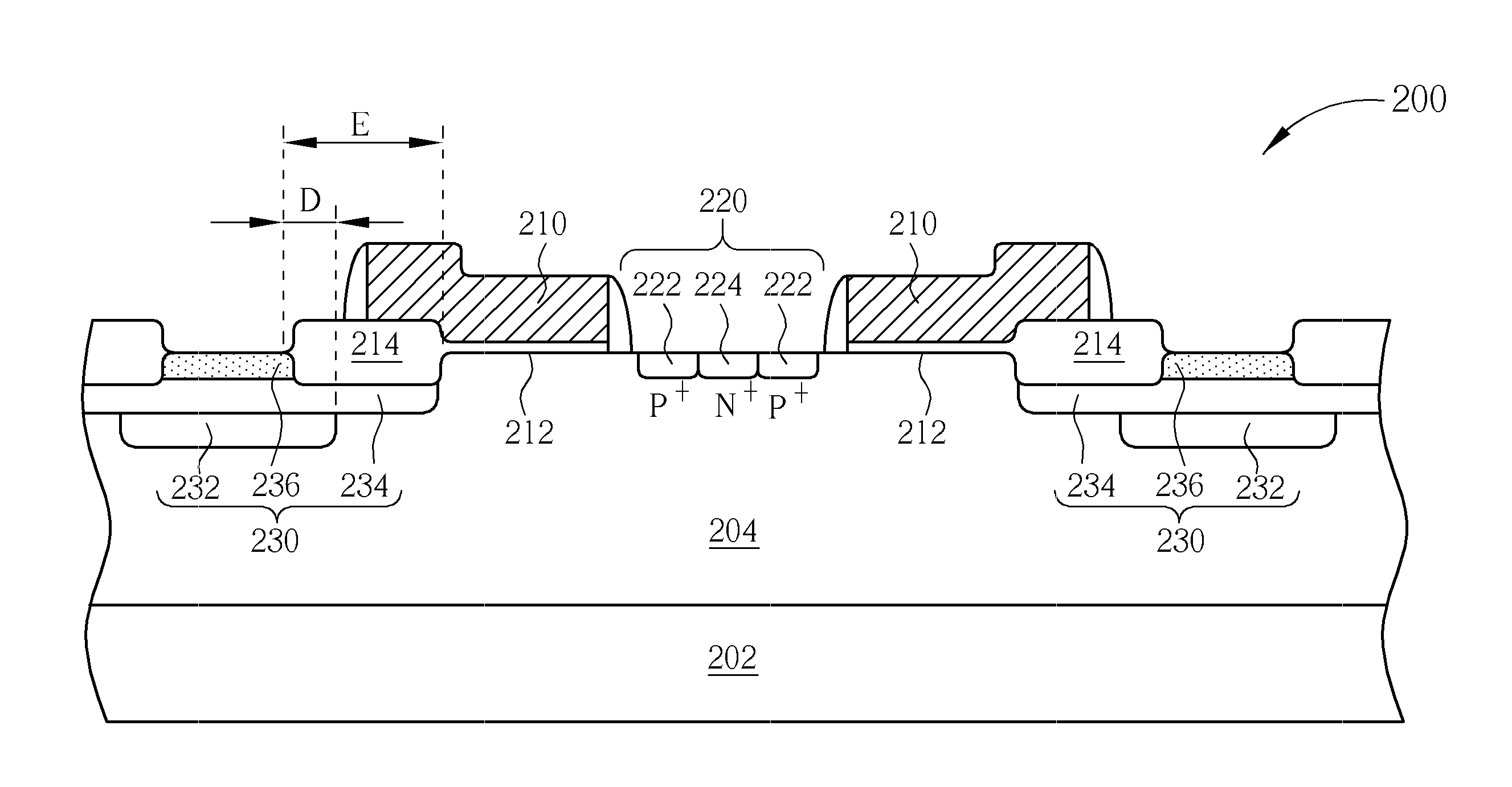
[0018]Please refer to FIGS. 4-6, FIG. 4 is a schematic drawing illustrating a LDMOS device provided by a preferred embodiment of the present invention, FIG. 5 is a cross-sectional view taken along a crossing line B-B′ in FIG. 4, and FIG. 6 is a schematic drawing illustrating a modification to the LDMOS device of the preferred embodiment. As shown in FIGS. 4-5, the LDMOS device 200 provided by the preferred embodiment includes a semiconductor substrate 202, which has a first conductive type, and a deep well region 204 having a second conductive type formed therein. In the preferred embodiment, the first conductive type is P-type and the second conductive type is N-type. However, those skilled in the art would easily realize that it is not limited to have the first conductive type being N-type and the second conductive type being P-type. Accordingly, the LDMOS device 200 provided by the preferred embodiment is a P-type LDMOS device positioned on an N-type deep well region 204 in a P-t...
PUM
 Abstract
Description
Claims
Application Information


