
Geometry of MOS device with low on-resistance

a technology of metal oxide semiconductors and geometries, applied in the direction of semiconductor devices, electrical apparatus, transistors, etc., can solve the problems of increasing manufacturing costs, less computing power in the same area of chips, and larger chips, so as to reduce the ron of the mos, increase the area of the mos, and increase the gate width

Inactive Publication Date: 2016-10-11
MARVELL ASIA PTE LTD
View PDF42 Cites 0 Cited by
  • Summary
  • Abstract
  • Description
  • Claims
  • Application Information

AI Technical Summary

Benefits of technology

This patent describes a structure for a MOS (metal-oxide-semiconductor) transistor that reduces the size of the transistor and improves its performance. By using a looped gate region, the MOS can have a wider gate without increasing its area. By arranging bulk regions around the gate region and separating the source regions, the amount of MOS area can be reduced. This allows more computing power in the same area or smaller chips, reducing manufacturing costs. Additionally, a channel region can be formed beneath the gate region to allow current to flow from each source region to the drain region. By arranging the bulk regions in corners of the substrate, the effective channel width can be maximized.

Problems solved by technology

An increased MOS area may result in chips with less computing power in the same area, or larger chips with increased manufacturing costs.

Method used


Image

  • Geometry of MOS device with low on-resistance
  • Geometry of MOS device with low on-resistance
  • Geometry of MOS device with low on-resistance

Examples


Embodiment Construction

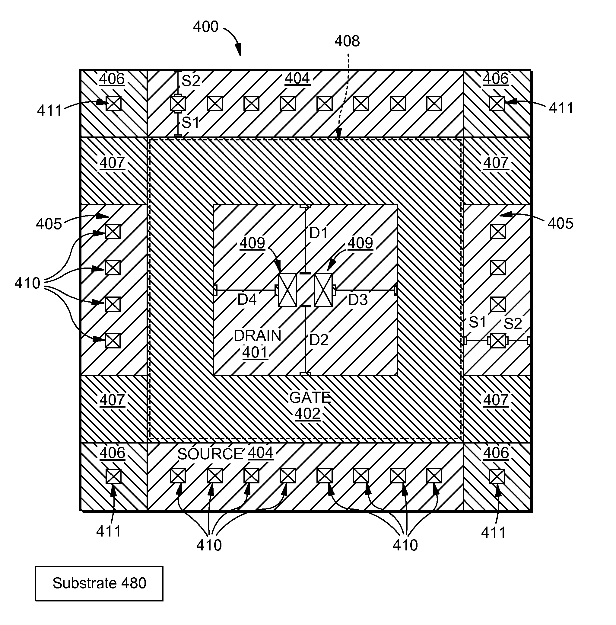
[0028]FIG. 4 is a diagram depicting a top view of a Metal Oxide Semiconductor (MOS) structure of a single MOS cell 400 in accordance with an embodiment of the invention. As illustrated in FIG. 4, cell 400 is formed in the shape of a square, but in other embodiments, cell 400 can have a circular shape or any multi-sided polygon shape, such as for example, a rectangle, a hexagon, or an octagon. Cell 400 can be, for example, a MOS transistor, including an n-type MOS (NMOS) and a p-type MOS (PMOS) transistor, and cell 400 can be a SQDMOS. Cell 400 includes at least a drain region 401, a gate region 402, source regions 404 and 405, and bulk regions 406 formed on a substrate, such as, for example, a silicon substrate, or any other suitable type of substrate.

[0029]FIG. 4 schematically illustrates a substrate 480, on which the drain region 401, the gate region 402, the source regions 404 and 405, and the bulk regions 406 are formed. FIG. 4 illustrates the top view of the single MOS cell 400...


PUM


Abstract

A Metal Oxide Semiconductor (MOS) device formed on a substrate and a method for forming the MOS device. The MOS device includes a drain region, a gate region surrounding the drain region, source regions arranged around the gate region and across from the drain region, and bulk regions arranged around the gate region and separating the source regions. The gate region is formed in a loop around the drain region. In this manner, the on-resistance (Ron) of a MOS device is decreased without also increasing the area of the MOS device.

Description

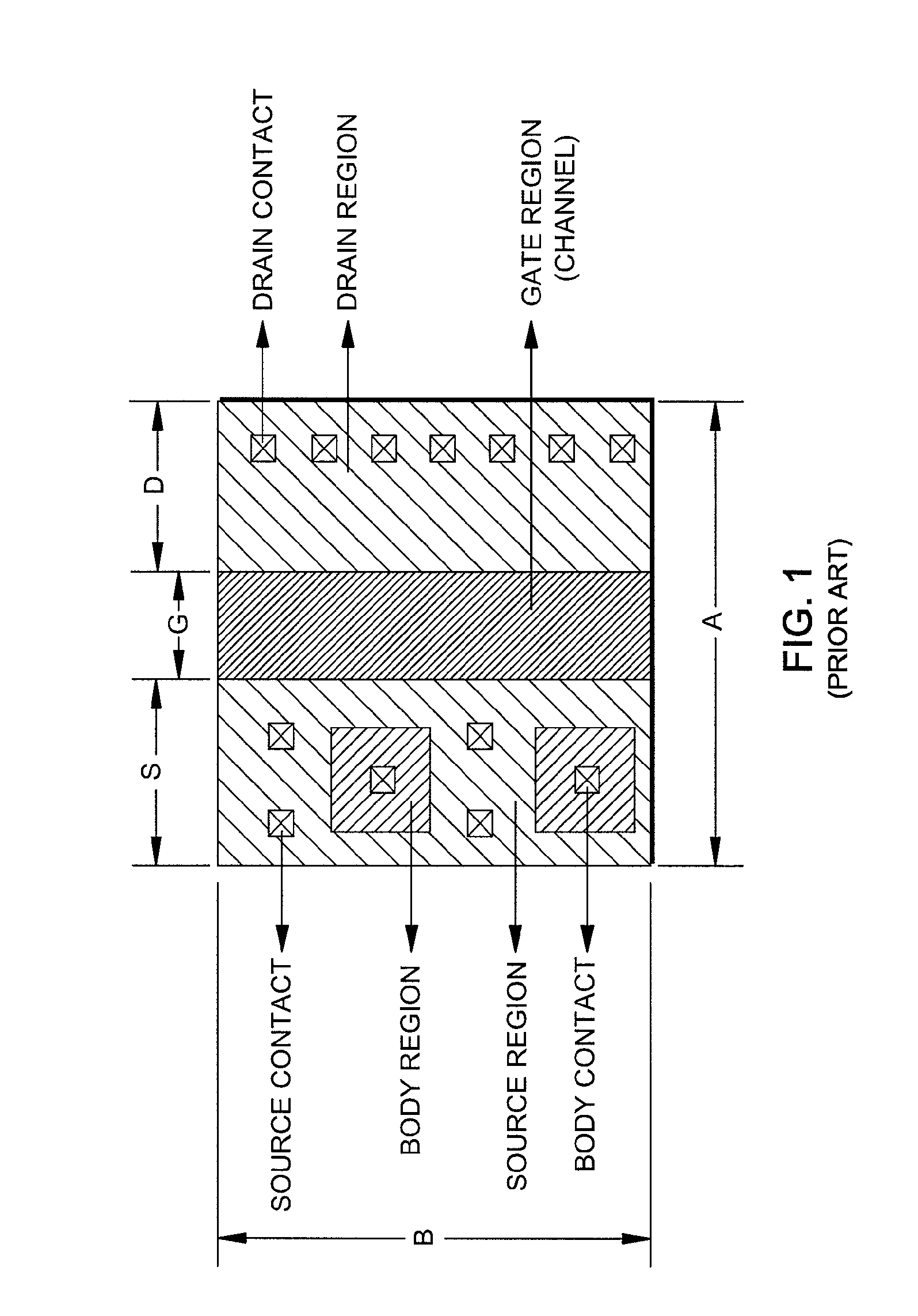
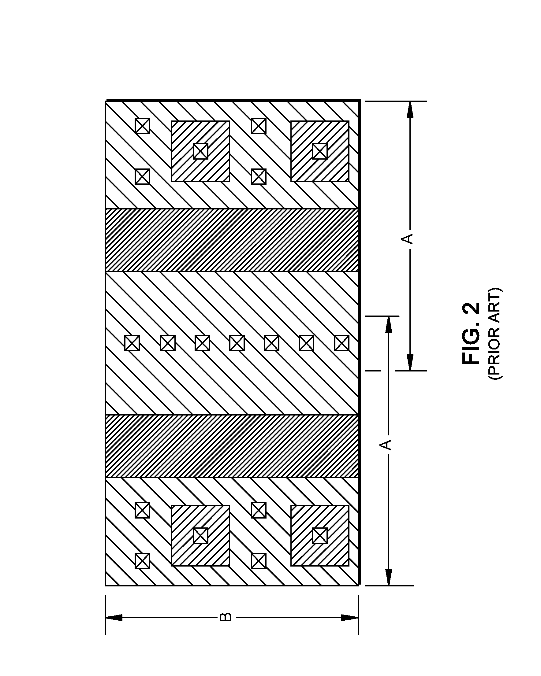
CROSS-REFERENCE TO RELATED APPLICATION[0001]This application claims the benefit of U.S. Provisional Patent Application No. 60 / 882,250, filed Dec. 28, 2006, the contents of which are hereby incorporated by reference as if fully stated herein.FIELD OF THE INVENTION[0002]The present invention relates to the geometry of a Metal Oxide Semiconductor (MOS) device, so as to produce a device having a low on-resistance, and particularly to a Square-Double-diffused Metal Oxide Semiconductor (SQDMOS) device with such a geometry.BACKGROUND OF THE INVENTION[0003]For comparison purposes, FIG. 1 shows a top view of the geometry of a conventional Metal Oxide Semiconductor (MOS) structure with gate, drain, source, and body (bulk) regions. The width of the MOS channel (gate region) is B and the length of the MOS channel is G. The lengths of the source and drain regions, S and D, respectively, are based on design rules of a particular process technology to achieve certain reliability and voltage capabi...

Claims


Application Information

Patent Timeline
Patent Type & Authority Patents(United States)
IPC IPC(8): H01L29/66H01L21/8234H01L27/02H01L27/088H01L29/78H01L29/423H01L29/06H01L29/417
CPCH01L27/0207H01L21/823437H01L27/088H01L29/0692H01L29/0696H01L29/4238H01L29/78H01L29/7835H01L29/41725H01L29/41758
Inventor SUTARDJA, SEHATKRISHNAMOORTHY, RAVISHANKER
Owner MARVELL ASIA PTE LTD
Learn More