
System and method for bit-wise selective masking of scan vectors for X-value tolerant built-in self test

a built-in self test and scan vector technology, applied in the direction of electronic circuit testing, measurement devices, instruments, etc., can solve the problems of inability to suitably address on-going ic validation, inability to continuously validate the ic used as a brake controller in an automobile, and inability to provide suitable measures in the past. to achieve the effect of maximizing ic coverage and reliability

Active Publication Date: 2016-09-20
CADENCE DESIGN SYST INC
View PDF13 Cites 25 Cited by
  • Summary
  • Abstract
  • Description
  • Claims
  • Application Information

AI Technical Summary

Benefits of technology

The present invention provides a solution to improve the coverage and reliability of an integrated circuit (IC) during verification. This solution involves selectively optimizing the masking of individual bits in the IC. The technical effect is to enhance the efficiency and accuracy of the verification process.

Problems solved by technology

Previous attempts in the art have not provided suitable measures.
However, such an approach requires complicated physical mating or probing by testing equipment in clean room environments to each port of an IC and fails to suitably address on-going IC validation after deployment in the field with changing operational circumstances such as clock speed.
For example, an IC used as a brake controller in an automobile cannot be continuously validated once the external testing apparatus has been disconnected and the IC has left the clean-room.

Method used


Image

  • System and method for bit-wise selective masking of scan vectors for <i>X</i>-value tolerant built-in self test
  • System and method for bit-wise selective masking of scan vectors for <i>X</i>-value tolerant built-in self test
  • System and method for bit-wise selective masking of scan vectors for <i>X</i>-value tolerant built-in self test

Examples


Embodiment Construction

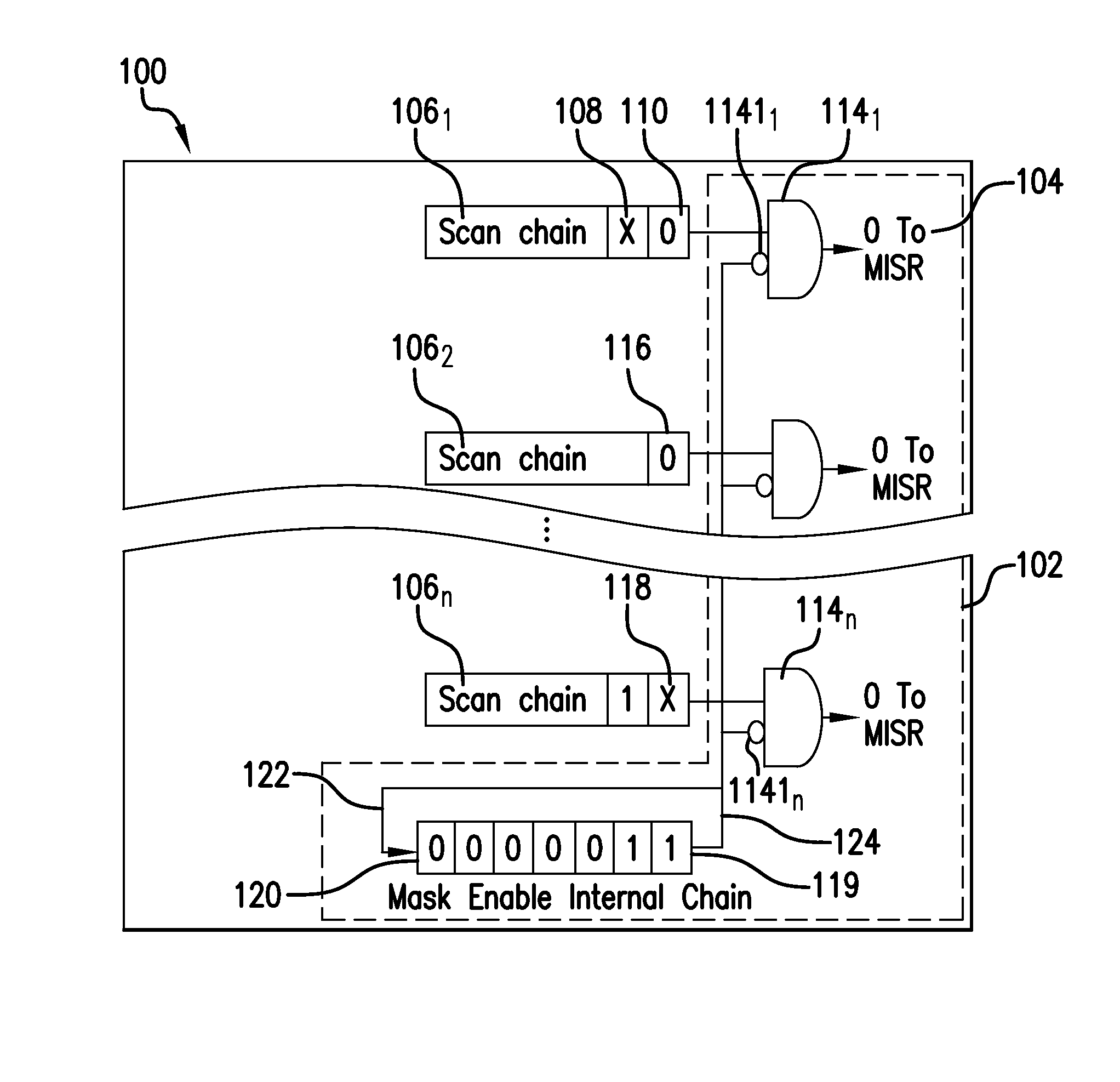
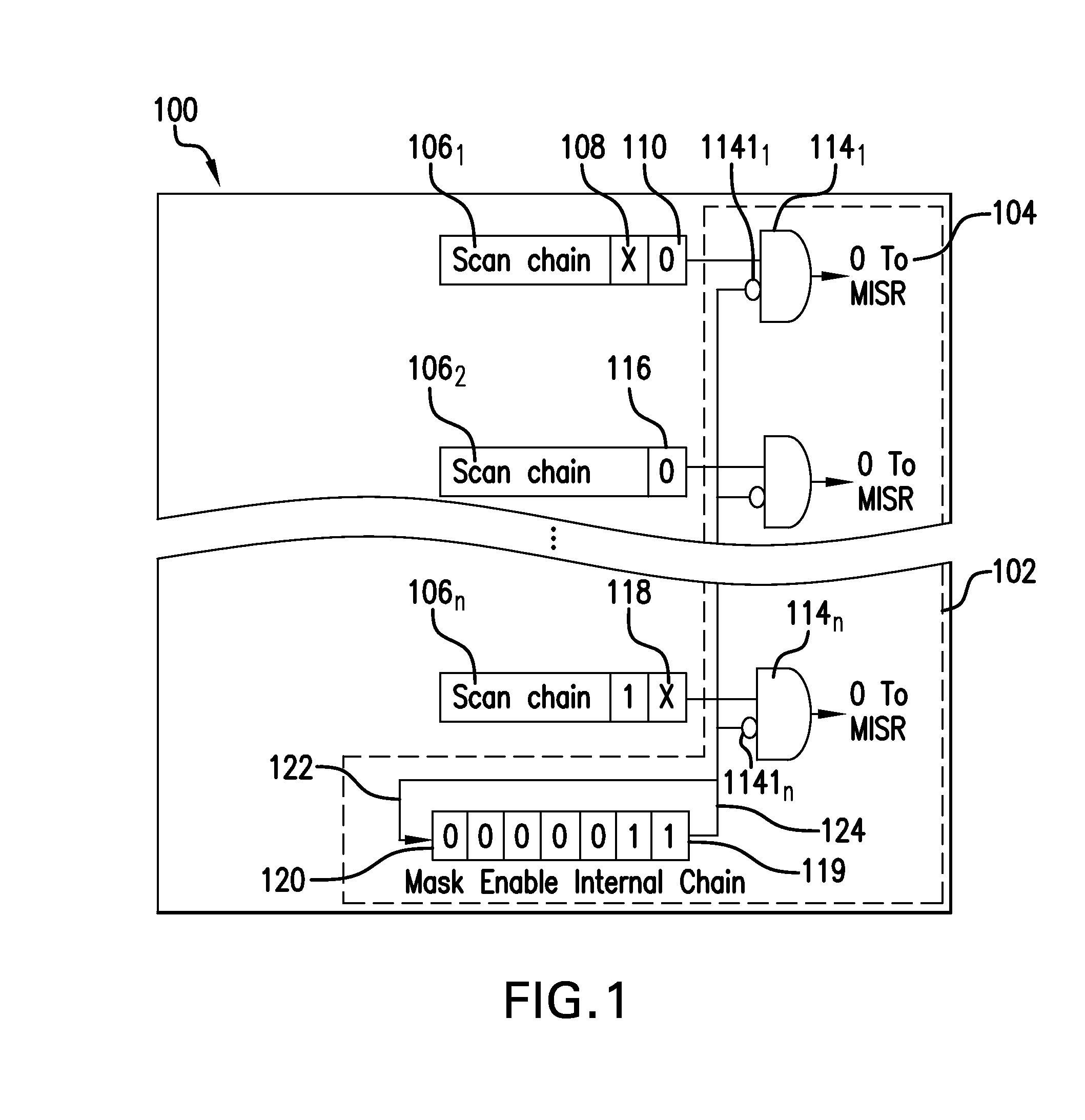
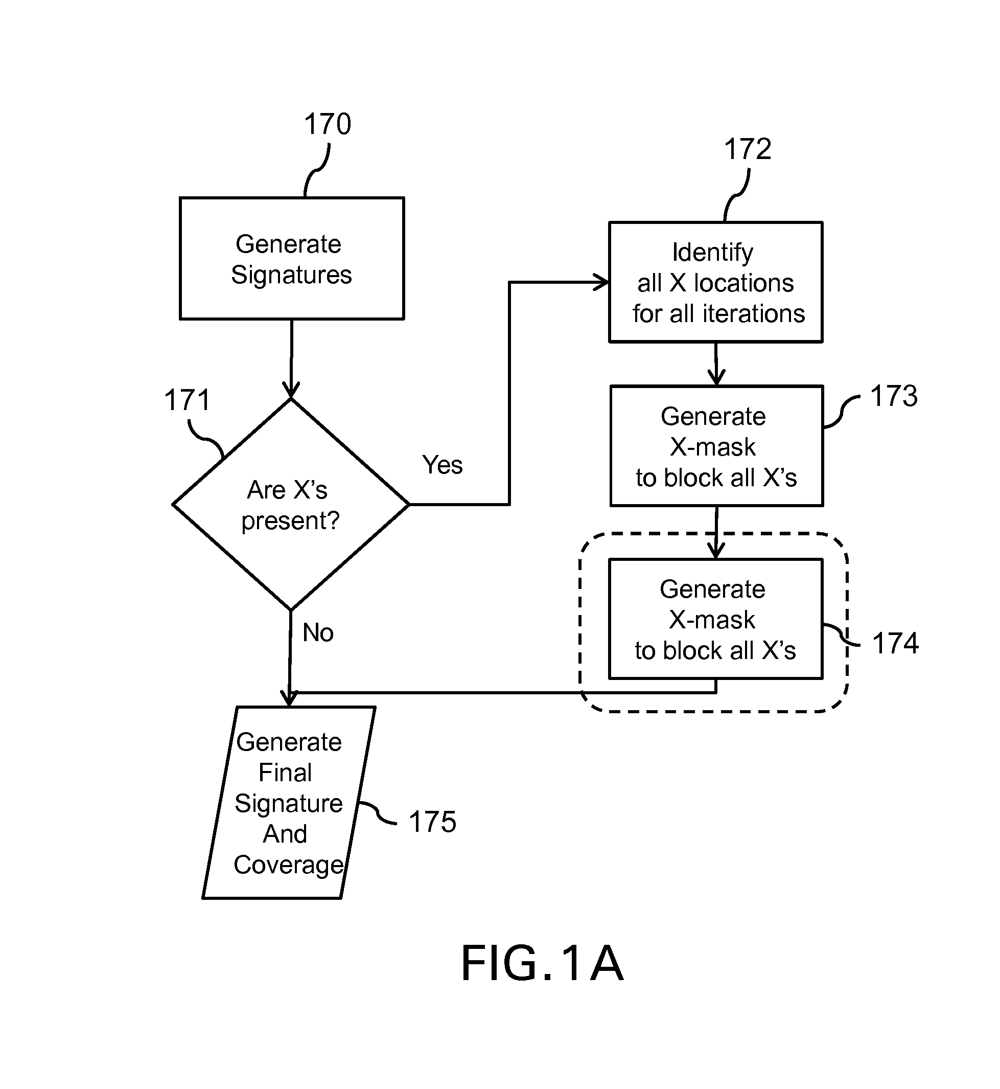
[0022]The subject system and method provide for selective bit-wise masking of operational scan results generated from a built-in self-test (BIST) incorporated into an integrated circuit (IC). The subject system and method provide for a BIST which is tolerant of X-values (which may be unknown, indeterminate, out of bound, or other unexpected values—as opposed to standard expected values such as “0” and “1”). Such X-values may appear in the operational scan results of the IC. X-values may be the result of un-modeled logic, tri-stated or floating busses, timing violations, un-driven nets, non-initialized flip-flops or latches, and the like. A composite mask pattern is selectively generated according to identified locations of these X-values in scanned flip flops, registers, or memory elements of the IC during a simulation of that IC. The composite mask pattern is cyclically maintained through repeated bit-wise shifts with recycling of bits from a least significant bit position to a mos...


PUM


Abstract

A system and method are provided for selective bit-wise masking of X-values in scan channels in an integrated circuit (IC) during a built-in self test (BIST). The composite mask pattern is selectively generated according to locations of X-values identified in a simulation of the IC. The composite mask pattern is stored on the IC and cyclically maintained while being applied to the operational scan results of the IC. The composite mask pattern is recycled over a plurality of scan iterations to effectively prevent the X-values from influencing the resulting signature of the BIST that represents a functional fingerprint of the IC and minimize storage requirements for the composite mask pattern.

Description

BACKGROUND OF THE INVENTION[0001]The present invention is generally directed to a system and method for built-in self test (BIST) of a fabricated Integrated Circuit (IC) device to ensure proper operation thereof. With steadily increasing IC complexity, fabrication quantities, and IC reliance, there is an ever increasing need to verify proper operation of ICs without overly burdensome time and equipment requirements. Moreover, these verification measures should tolerate some uncertainties in the IC and yet still provide assurance of proper operation. Further still, verification measures should be resilient to changing operational parameters encountered after fabrication. Previous attempts in the art have not provided suitable measures.[0002]Attempts have been made in the art within the fabrication and packaging facilities themselves to physically connect external automated testing equipment (ATEs) to input and output ports of ICs to stream known inputs and measure the outputs of the ...

Claims


Application Information

Patent Timeline
Patent Type & Authority Patents(United States)
IPC IPC(8): G01R31/3185G01R31/3177G01R31/317G01R31/3183
CPCG01R31/318335G01R31/31703G01R31/3177G01R31/318566G01R31/318536G01R31/318563G01R31/318547
Inventor MEEHL, DALE EDWARD
Owner CADENCE DESIGN SYST INC
Learn More