
Organic light emitting diode display device

a light-emitting diode and display device technology, applied in the field of organic light-emitting diodes (oled) display devices, can solve the problems of low life span, limited use of passive matrix types, and non-uniform brightness of oled display devices, so as to minimize the threshold voltage variation of driving transistors and minimize the lowering of the aperture ratio of each pixel.

Active Publication Date: 2016-09-20
SAMSUNG DISPLAY CO LTD
View PDF53 Cites 0 Cited by
  • Summary
  • Abstract
  • Description
  • Claims
  • Application Information

AI Technical Summary

Benefits of technology

The present invention is about an OLED display device that can minimize the difference in voltage between driving transistors, prevent the aperture ratio of pixels from decreasing, and ensure that each pixel's OLED receives the optimal driving current, even if data signals have the same voltage.

Problems solved by technology

Although the passive matrix type is easily manufactured as its display area is simply formed by an anode and a cathode in a matrix, the use of the passive matrix type is limited to small displays due to low resolution, a high driving voltage, low life-span of materials, etc.
The OLED display devices have a specific variation in threshold voltage of a TFT in each pixel during a fabrication process of the TFT, which results in a non-uniform brightness of the OLED display device.
However, the OLED display device having such a compensation circuit requires several TFTs to form the compensation circuit, thereby requiring complicated pixel circuits which decrease a light emitting area due to a reduction in aperture ratio of each pixel.
Also, a voltage range of the data signal is also increased, and thus the data driving unit is complicated and power consumption increases.

Method used


Image

  • Organic light emitting diode display device
  • Organic light emitting diode display device
  • Organic light emitting diode display device

Examples


Embodiment Construction

[0021]Reference will now be made in detail to the present embodiments of the present invention, examples of which are illustrated in the accompanying drawings, wherein like reference numerals refer to the like elements throughout. The embodiments are described below in order to explain the present invention by referring to the figures. In the drawings, length and thickness of the layers and regions may be exaggerated for clarity. Also, like numerals denote like components, and when a part is described as being “connected” with a part, the part may be “directly connected” or “electrically connected” with the part and / or a third part may be interposed therebetween.

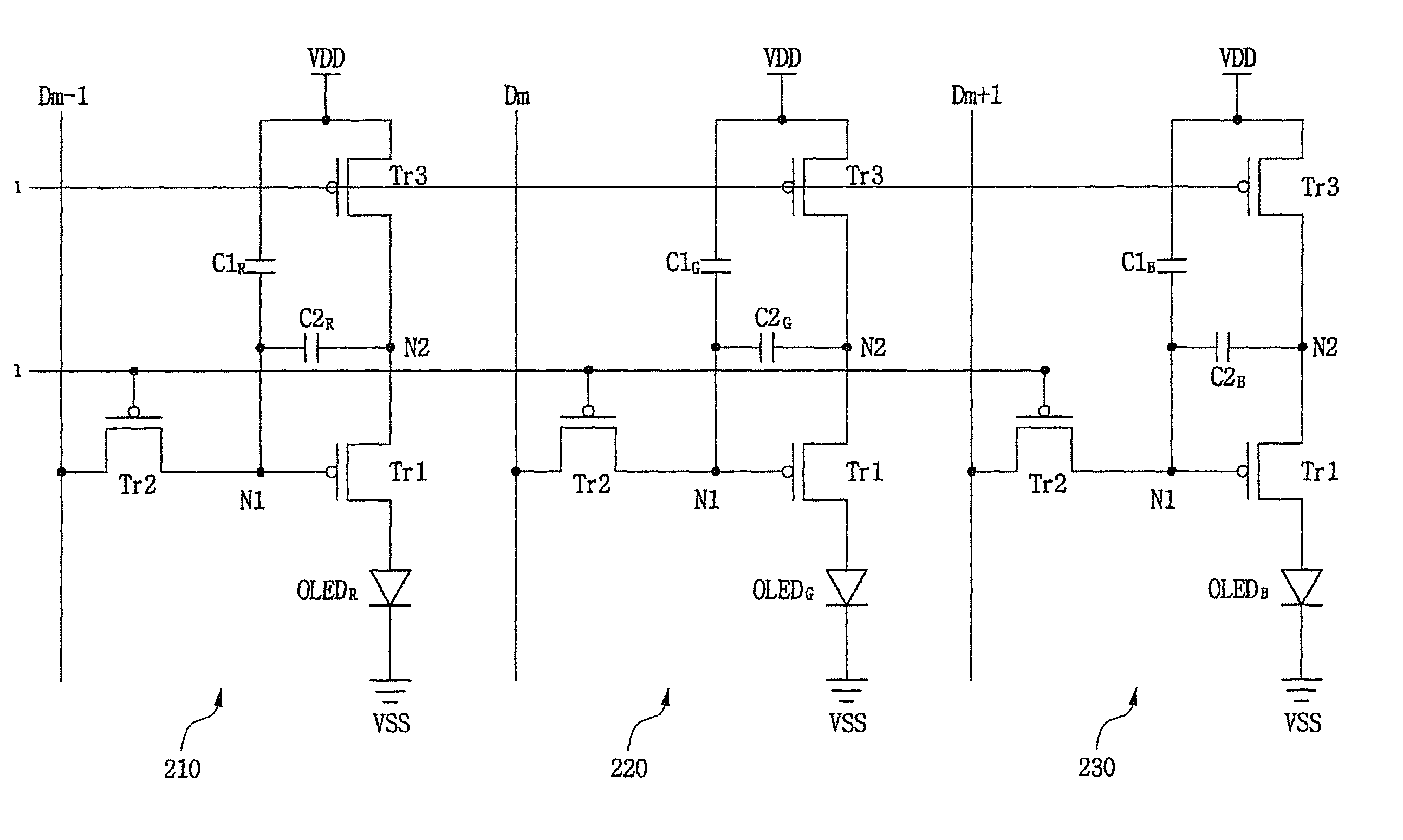
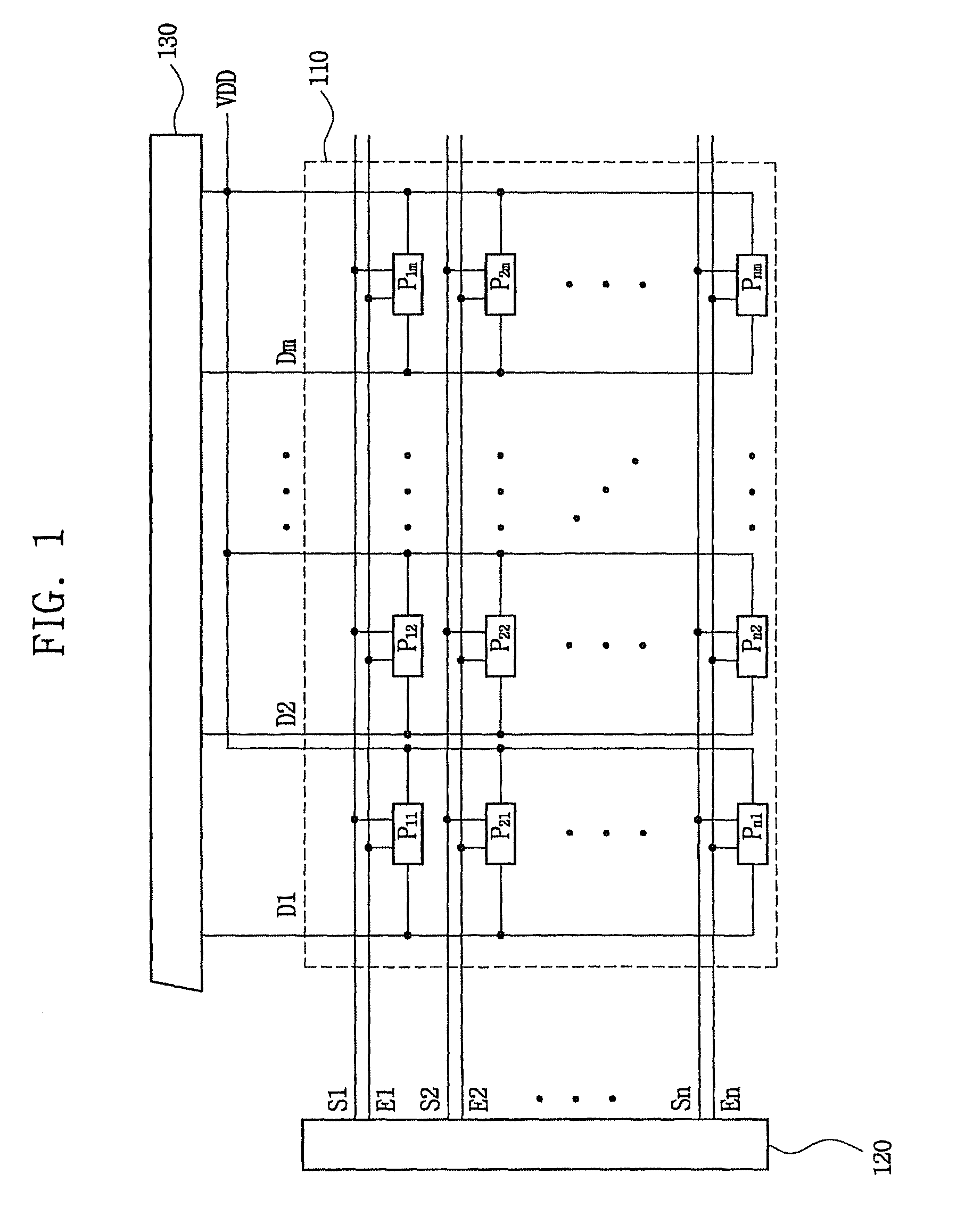
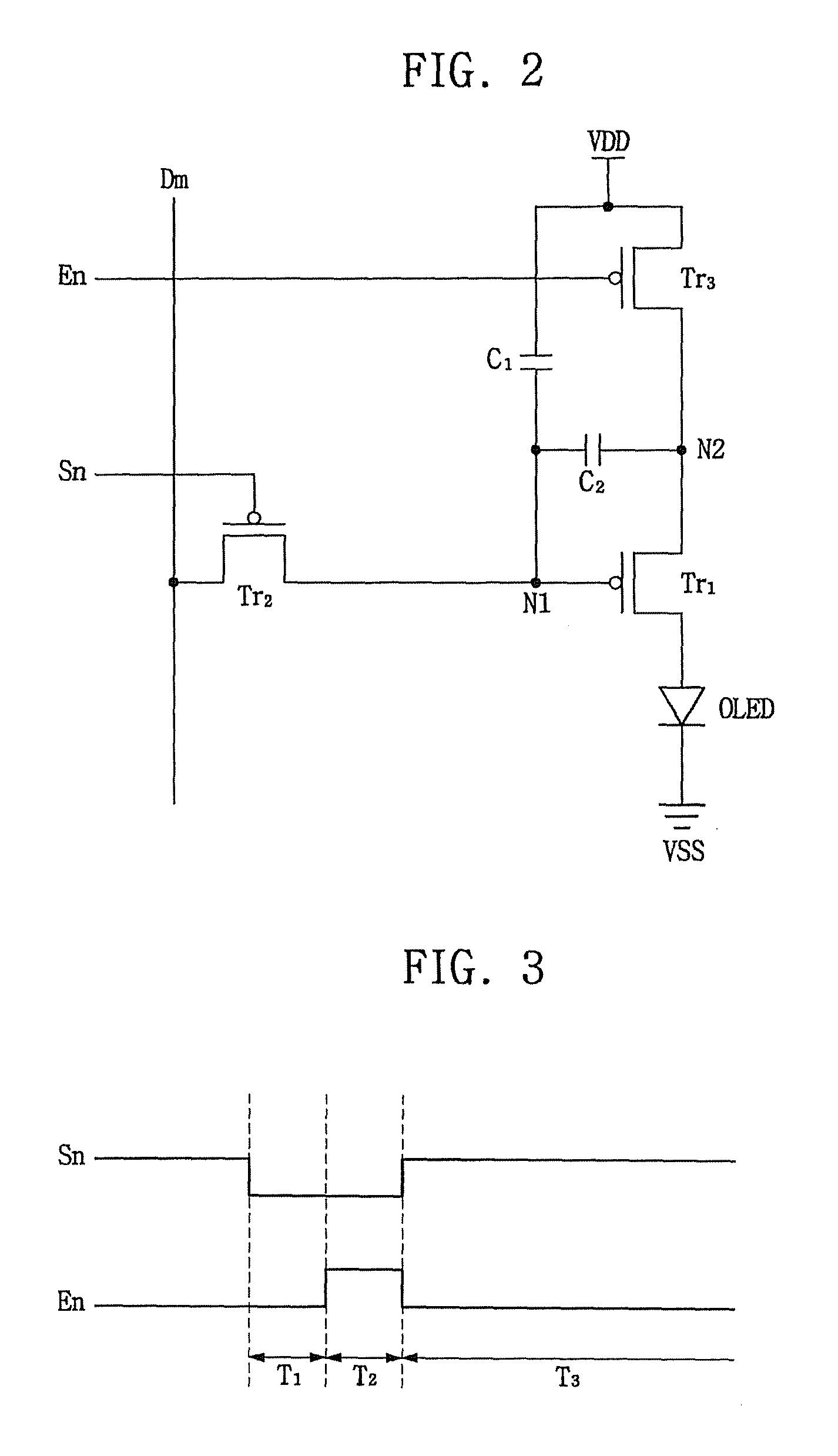
[0022]FIG. 1 is a block diagram of an organic light emitting diode (OLED) display device according to an exemplary embodiment of the present invention. Referring to FIG. 1, the OLED display device according to this exemplary embodiment of the present invention includes a pixel unit 110 having a plurality of pixels P11˜Pnm, a...


PUM


Abstract

An organic light emitting diode (OLED) display device minimizes a threshold voltage variation of a drive transistor in a pixel circuit, increases an aperture ratio, and minimizes power consumption by applying a same range of data voltages to respective pixels. The OLED display device includes a first capacitor electrically connected between a first node and a power supply line; and a second capacitor electrically connected between the first node and a second node, wherein capacitances of the first and second capacitors are different from each other and adjustable.

Description

CROSS-REFERENCE TO RELATED APPLICATION[0001]This application claims the benefit of Korean Patent Application No. 2007-61257, filed Jun. 21, 2007, the disclosure of which is hereby incorporated herein by reference.BACKGROUND OF THE INVENTION[0002]1. Field of the Invention[0003]Aspects of the present invention relate to an organic light emitting diode (OLED) display device capable of minimizing a threshold voltage variation of a driving transistor in a pixel circuit, minimizing lowering of an aperture ratio, and minimizing power consumption by applying the same range of data voltages to respective pixels.[0004]2. Description of the Related Art[0005]Flat panel display devices, for example, liquid crystal display devices and organic light emitting diode (OLED) display devices, are lightweight and thin and are widely used as alternatives to cathode ray tube (CRT) display devices. Among these flat panel display devices, OLED display devices, in particular, have attracted considerable atte...

Claims


Application Information

Patent Timeline
Patent Type & Authority Patents(United States)
IPC IPC(8): G09G3/3208G09G3/32
CPCG09G3/3233G09G3/3291G09G2300/0465G09G2300/0819G09G2300/0852G09G2300/0861G09G2310/0297G09G2320/0233G09G2330/021G09G3/20G09G3/30G09G3/32H05B33/12
Inventor LEE, JAE-YONGKIM, YANG-WAN
Owner SAMSUNG DISPLAY CO LTD
Learn More