Nitrogen implementation to minimize device variation

a technology of nitrogen and device variation, applied in the field of semiconductor processing, can solve the problems of reducing yield, oxynitride layer thickness, and unsatisfactory reduction of transistor threshold voltage (vt), and achieve the effect of constant threshold voltage characteristics

Inactive Publication Date: 2005-01-25
INTEGRATED DEVICE TECH INC
View PDF0 Cites 2 Cited by
  • Summary
  • Abstract
  • Description
  • Claims
  • Application Information

AI Technical Summary

Benefits of technology

The invention provides a method for creating an oxynitride layer having constant threshold voltage characteristics. By introducing a nitrogen concentration gradient into the oxynitride layer, the threshold voltage variations that would normally be introduced by a thickness gradient in the oxynitride layer can be minimized.

Problems solved by technology

This “dopant penetration” results in an undesirable reduction in transistor threshold voltage (Vt).
Unfortunately, conventional RTN chambers produce oxynitride layers having thicknesses that increase in the process gas (i.e., N2O) flow direction.
This in turn can lead to reduced yield and / or increased production costs as process parameters are tightened to compensate for this threshold voltage variation.

Method used


Image

  • Nitrogen implementation to minimize device variation
  • Nitrogen implementation to minimize device variation
  • Nitrogen implementation to minimize device variation

Examples


Embodiment Construction

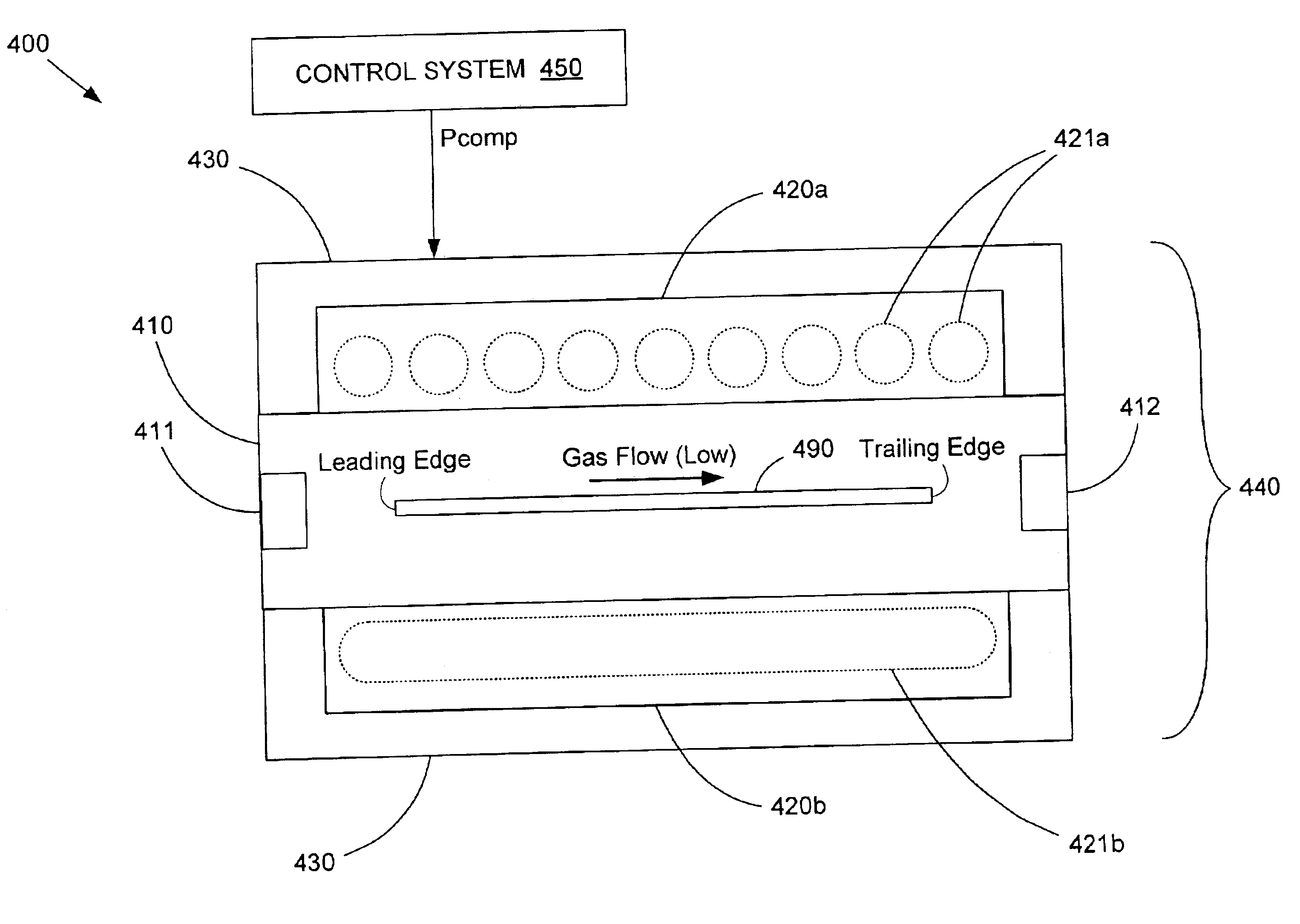
The invention provides a method for ensuring consistent PMOS transistor performance across a processed wafer when an RTN process is used in the formation of the PMOS transistor gate dielectrics. By introducing a nitrogen concentration gradient into the oxynitride layer formed during the RTN process, effects on threshold voltage caused by a thickness gradient in the oxynitride layer can be minimized. FIG. 4 shows an RTN system 400 configured to create a nitrogen concentration gradient in an oxynitride layer. RTN system 400 comprises a control system 450 that provides a PMOS compensation recipe Pcomp to an RTN process chamber 440. RTN process chamber 440 comprises a quartz isolation tube 410 that includes a gas inlet port 411 and a gas outlet port 412. RTN process chamber 440 further includes heat sources 420a and 420b, which can comprise any means for heating a semiconductor (e.g., silicon) wafer 490 in isolation tube 410. For example, optional tungsten halogen lamps 421a and 421b ca...


PUM


Abstract

A rapid thermal nitridation (RTN) process produces a nitrogen concentration gradient in an oxynitride layer to compensate for transistor threshold voltage effects from a thickness gradient in the oxynitride layer. The nitrogen concentration gradient is selected to allow greater dopant penetration through thicker gate dielectrics in PMOS transistors formed using the oxynitride layer. Any increases in threshold voltage due to thicker gate dielectrics are counteracted by corresponding decreases in threshold voltage due to dopant penetration, allowing consistent threshold voltage values to be maintained for all PMOS transistors on a single wafer. The nitrogen concentration gradient can be introduced by regulating the flow of nitrous oxide during RTN processing to cause an accumulation of atomic oxygen to develop within the process chamber. The atomic oxygen forms a concentration distribution that increases in the direction of nitrous oxide flow, and therefore removes incorporated nitrogen from the oxynitride layer in corresponding proportions.

Description

BACKGROUND OF THE INVENTION1. Field of the InventionThe present invention relates to the area of semiconductor processing. In particular, the present invention relates to a method for minimizing device variation across a wafer by adjusting oxynitride layer nitrogen concentration during rapid thermal nitridation.2. Discussion of Related ArtThe dimensions of modern semiconductor devices are continually being reduced to improve integrated circuit (IC) capabilities while increasing speed and decreasing power consumption. To accommodate this continual trend towards greater miniaturization, the semiconductor processes used in the production of ICs are constantly being refined. One area of critical importance is the formation of the gate dielectrics in metal-oxide-semiconductor (MOS) transistors—in particular the gate dielectrics of PMOS transistors. Historically, silicon dioxide (SiO2) has been the material of choice for PMOS transistor gate dielectrics. However, as the thickness of an Si...

Claims


Application Information

Patent Timeline
Patent Type & Authority Patents(United States)
IPC IPC(8): H01L21/02H01L21/28H01L21/70H01L21/314H01L21/8238H01L21/8234H01L29/51
CPCH01L21/28202H01L21/3144H01L21/823412H01L29/518H01L21/823807H01L21/823857H01L21/823462H01L21/02255H01L21/02247
Inventor AHN, JAE-GYUNGWOO, YOUNG T.
Owner INTEGRATED DEVICE TECH INC
Why Eureka
Try Eureka