Semiconductor memory device, method of controlling read preamble signal thereof, and data transmission system

a memory device and read preamble technology, applied in the direction of information storage, static storage, digital storage, etc., can solve the problems of internal clock phase delay with regard to ck signal, difficult to detect read preamble signal with suitable timing to receive head data, and dll off mode is hardly used

Active Publication Date: 2016-10-11
LONGITUDE LICENSING LTD
View PDF1 Cites 0 Cited by
  • Summary
  • Abstract
  • Description
  • Claims
  • Application Information

AI Technical Summary

Benefits of technology

[0015]However, since it is not possible to adjust the phase of an internal clock so that the phase of the CK signal matches the phase of the DQS signal, by the DLL circuit as in the DLL ON mode, the internal clock has a phase delay with regard to the CK signal. This phase delay appears as a phase delay time tDQSCK (DLL OFF mode) of the DQS signal with respect to the CK signal, and a numerical value thereof is 2000 ps to 5000 ps approximately. That is, the tDQSCK (DLL OFF mode) is a number larger by an order of magnitude or more than a tDQSCK (DLL ON mode) when the DLL is ON as described already, and since an internal clock necessarily has a phase delay with respect to the CK signal provided from outside, there is a difference in that the tDQSCK (DLL OFF mode) is a positive number. As may be understood easily from FIG. 3, for a tDQSCKmin where the phase delay is smallest, a read preamble time-period is already ended, and at timing at which a toggle operation is entered, for a tDQSCKmax where the phase delay is largest, it is still before transmission of the read preamble.
[0016]In this type of case, there exists no timing at which the read preamble signal can be assuredly detected even when the delay time-period of a DDR SDRAM such as timing from ts to te as shown in FIG. 1 varies. In this type of case, the memory controller cannot normally read the read data, in control flow shown in FIG. 2

Problems solved by technology

However, since there are various problems in semiconductor memory devices using a high speed data transfer rate as in the DDR3 SDRAM, it is considered that in actuality the DLL OFF mode is hardly used.
One reason for this is that, as described below, with conventional memory controllers, it is difficult to detect a read preamble signal with suitable timing to receive head data of read data without error.
However, since it is not possible to adjus

Method used


Image

  • Semiconductor memory device, method of controlling read preamble signal thereof, and data transmission system
  • Semiconductor memory device, method of controlling read preamble signal thereof, and data transmission system
  • Semiconductor memory device, method of controlling read preamble signal thereof, and data transmission system

Examples


example 1

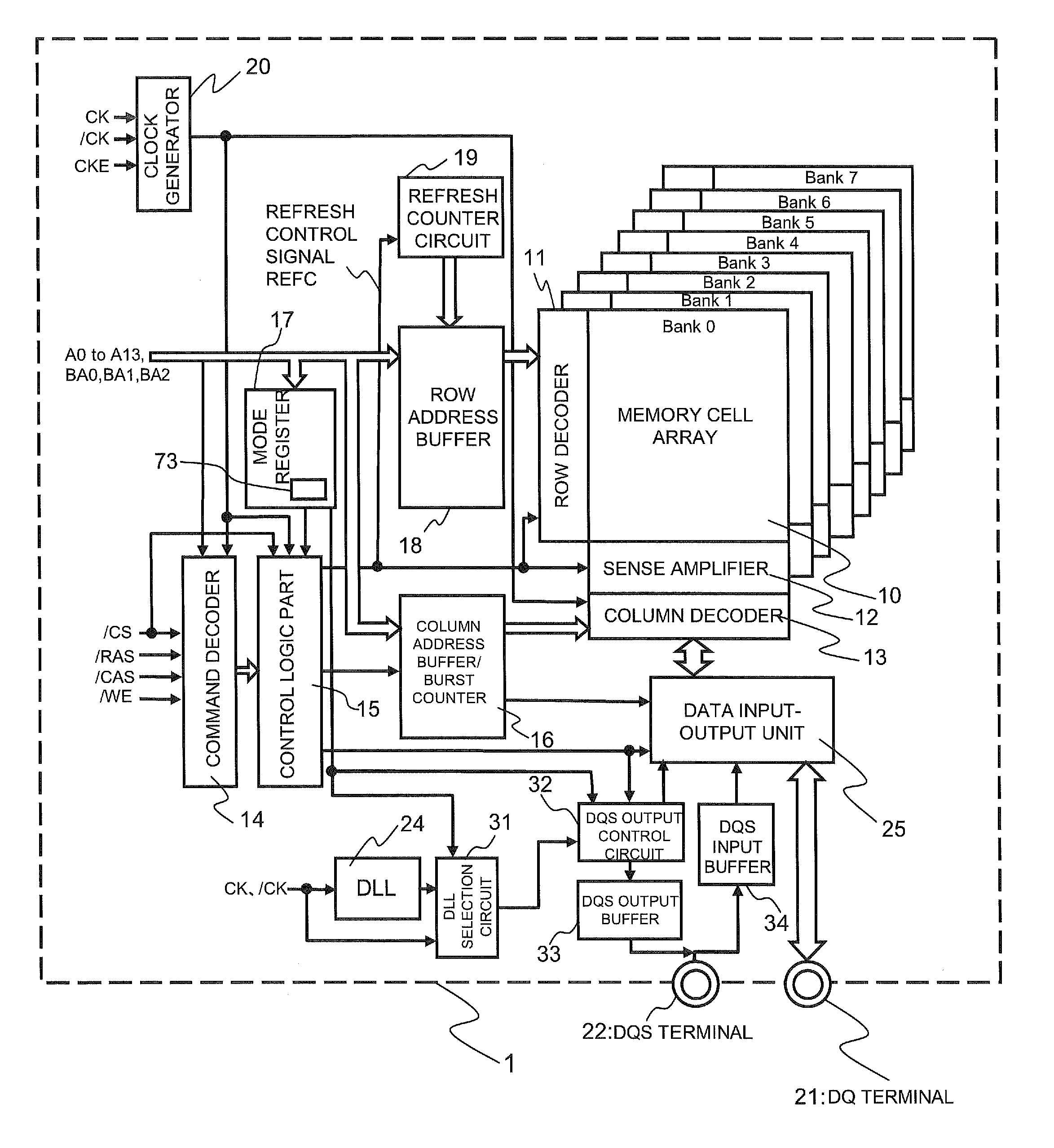
[0045]FIG. 5 is a configuration diagram of an overall memory system according to an example of the present invention. FIG. 5 is a 64-bit parallel read-write memory system. A semiconductor memory device 1 is an 8-bit parallel read-write device, and 8 semiconductor memory devices 1 are connected in parallel to perform 64-bit parallel reading and writing. Furthermore, in the memory system of FIG. 5 a configuration is assumed in which 2 ranks of the semiconductor memory devices 1 are mounted on each of two DIMMs (Dual Inline Memory Module). That is, the configuration is of a total of 4 ranks of semiconductor memory devices, DIMM1 Rank-1, DIMM1 Rank-2, DIMM2 Rank-1, DIMM2 Rank-2, and each rank further includes 8 semiconductor memory devices 1. The total number of semiconductor memory devices 1 mounted is 4 (ranks)×8=32. In FIG. 5, only 3 semiconductor memory devices 1 among the 8 semiconductor memory devices 1 that are connected in parallel are illustrated. Signals that control these 32 ...


PUM


Abstract

A system, includes a controller comprising a plurality of first external terminals configured to supply a command and an address, and communicate a data, and communicate a strobe signal related to the data; and a semiconductor memory device including a plurality of second external terminals corresponding to the plurality of first external terminals, at least one of the plurality of first external terminals and at least one of the plurality of second external terminals each being capable of supplying an information specifying a length of a preamble of the strobe signal before the semiconductor memory device communicates the data between the controller and the semiconductor memory device, the semiconductor memory device further including a preamble register configured to be capable of storing the information.

Description

REFERENCE TO RELATED APPLICATION[0001]The present application is a Continuation Application of U.S. patent application Ser. No. 14 / 940,692, filed on Nov. 13, 2015, which is a Continuation Application of U.S. patent application Ser. No. 14 / 738,764, filed on Jul. 12, 2015, now U.S. Pat. No. 9,208,852 which issued on Dec. 8, 2015, which is a Continuation Application of U.S. patent application Ser. No. 14 / 518,797, filed on Oct. 20, 2014, now U.S. Pat. No. 9,082,482 which issued on Jul. 14, 2015, which is a Continuation Application of U.S. patent application Ser. No. 13 / 832,448, filed on Mar. 15, 2013, now U.S. Pat. No. 8,867,252 which issued on Oct. 21, 2014, which is a Divisional Application of U.S. patent application Ser. No. 13 / 621,061, filed on Sep. 15, 2012, now U.S. Pat. No. 8,811,052 which issued on Aug. 19, 2014, which is a Continuation Application of U.S. patent application Ser. No. 13 / 465,826, filed on May 7, 2012, which is a Continuation Application of U.S. patent application...

Claims


Application Information

Patent Timeline
IPC IPC(8): G11C15/04G11C11/4076G11C11/4096
CPCG11C11/4076G11C11/4096G11C7/1051G11C7/1066G11C7/1072G11C7/22G11C7/222G11C8/18G11C11/409G11C15/00G11C15/04
Inventor KOSHIZUKA, ATSUO
Owner LONGITUDE LICENSING LTD
Why Eureka
Try Eureka