Semiconductor device, method of manufacturing the same, and method of forming multilayer semiconductor thin film

a semiconductor and thin film technology, applied in the direction of semiconductor devices, thermoelectric device junction materials, electrical apparatus, etc., can solve the problems of difficult, for example, to precisely adjust the physical properties according to processes, and low molecular design freedom, so as to improve and adversely affect the characteristics of semiconductor devices

Active Publication Date: 2013-03-19
SONY CORP
View PDF1 Cites 0 Cited by
  • Summary
  • Abstract
  • Description
  • Claims
  • Application Information

AI Technical Summary

Benefits of technology

[0011]It is desirable to provide a semiconductor device including a channel-forming region composed of a dioxaanthanthrene compound which provides high carrier mobility and high freedom of molecular design and which has excellent adaptability to processes, and a method of manufacturing the semiconductor device, and to provide a method of forming a multilayer semiconductor thin film including a semiconductor layer composed of a dioxaanthanthrene compound.
[0022]In semiconductor devices, the interface between the channel-forming region and the gate insulating layer has been considered as a region in which electric charges move, and is one of the most important parts that influence characteristics of semiconductor devices. Research has been conducted to improve characteristics of semiconductor devices by treating the surface of gate insulating layers using a surface-treating agent. For example, it has been reported that treatment of the surface of thermal oxide formed on the surface of a silicon substrate using an interface-treating agent, such as octadecyltrichlorosilane (OTS) or hexamethylenedisilazane (HMDS), improves characteristics of semiconductor devices. However, in such surface treatment, not only an additional treatment step is necessary, but also nano-scale irregularities may occur on the surface of gate insulating layers depending on treatment conditions, thus adversely affecting characteristics of semiconductor devices.
[0023]According to some embodiments of the present invention, a thin film is formed by application of a mixed solution including a polymeric insulating material and a dioxaanthanthrene compound having a specific structure, and subsequently the thin film is dried to induce phase separation of the polymeric insulating material and the dioxaanthanthrene compound having the specific structure, thereby forming a gate insulating layer from the polymeric insulating material and a channel-forming region from the dioxaanthanthrene compound having the specific structure. Alternatively, a thin film is formed by applying a mixed solution including a first material and a second material, and subsequently the thin film is dried to induce phase separation of the first material and the second material, thereby producing a stacked structure including a first layer composed of the first material and a second layer composed of the second material. Consequently, it is not necessary to perform surface treatment on the gate insulating layer or the first layer.
[0024]Moreover, in the dioxaanthanthrene compound according to any of the embodiments of the present invention suitable for forming semiconductor layers, the molecules pack in the pi-stacking arrangement in the neutral state in the absence of an applied voltage and in the ionic state in the presence of an applied voltage. Therefore, without introducing bulky substituents, the backbones of the dioxaanthanthrene compound according to any of the embodiments of the present invention can easily pack in the pi-stacking arrangement. Consequently, it is possible to increase the freedom of molecular design of an organic semiconductor material constituting semiconductor layers that exhibit high carrier mobility, and to facilitate molecular design. Moreover, adaptability to processes can be improved. That is, channel-forming regions can be formed by a wet process, such as coating or printing. Thereby, it is possible to easily produce organic semiconductor thin films having high carrier mobility as well as high stability, durability, and heat resistance, and high-performance semiconductor devices.

Problems solved by technology

However, in order to achieve packing of pentacene backbones in the pi-stacking arrangement, it is necessary to introduce bulky substituents as described above, which results in low freedom of molecular design.
Therefore, it is difficult, for example, to precisely adjust the physical properties according to processes.

Method used


Image

  • Semiconductor device, method of manufacturing the same, and method of forming multilayer semiconductor thin film
  • Semiconductor device, method of manufacturing the same, and method of forming multilayer semiconductor thin film
  • Semiconductor device, method of manufacturing the same, and method of forming multilayer semiconductor thin film

Examples


example 1

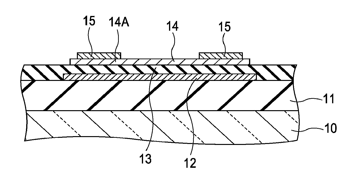
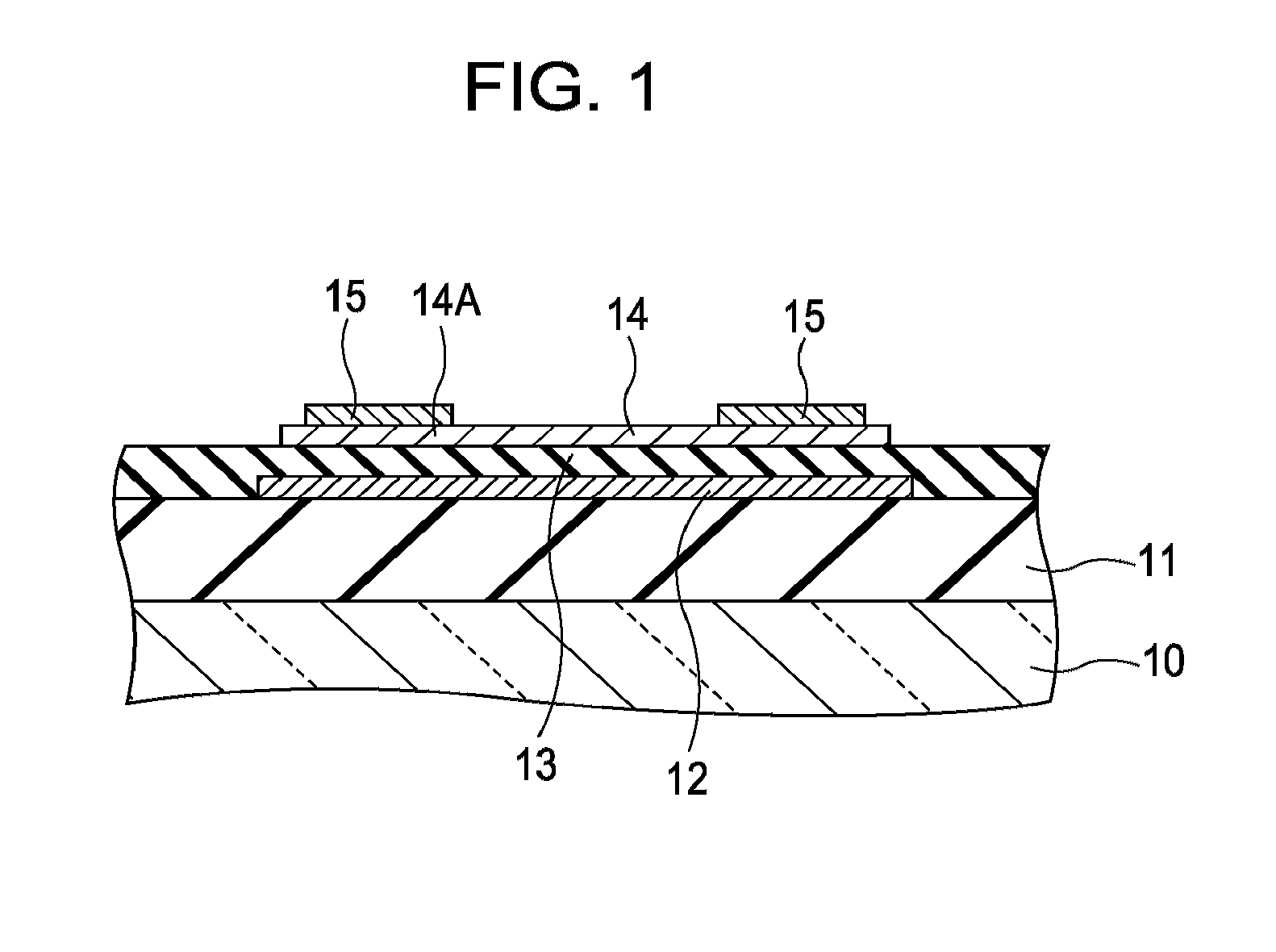
[0115]Example 1 relates to semiconductor devices according to the first and second embodiments of the present invention, methods of manufacturing the same, and methods of forming a multilayer semiconductor thin film according to the first and second embodiments of the present invention. A semiconductor device (specifically, field-effect transistor (FET), more specifically, thin-film transistor (TFT) of Example 1 includes a gate electrode, a gate insulating layer, source / drain electrodes, and a channel-forming region that are disposed on a base, in which the channel-forming region is composed of the dioxaanthanthrene compound represented by structural formula (1) described above, and the gate insulating layer is composed of PaMS, wherein at least one of R3 and R9 represents a substituent other than hydrogen. Furthermore, a semiconductor device of Example 1 includes a gate electrode, a gate insulating layer, source / drain electrodes, and a channel-forming region that are disposed on a ...

example 2

[0137]Example 2 is a modification of Example 1. In Example 2, as the dioxaanthanthrene compound, 3,9-bis(4-propylphenyl)-peri-xanthenoxanthene [PXX—(C3Ph)2] represented by structural formula (11) of Example 12 described later, in which R3 and R9 are each an aryl-alkyl group, was used. Tetralin was used as the solvent. The mixing ratio of PaMS to PXX—(C3Ph)2 was 1:1 (weight ratio).

[0138]

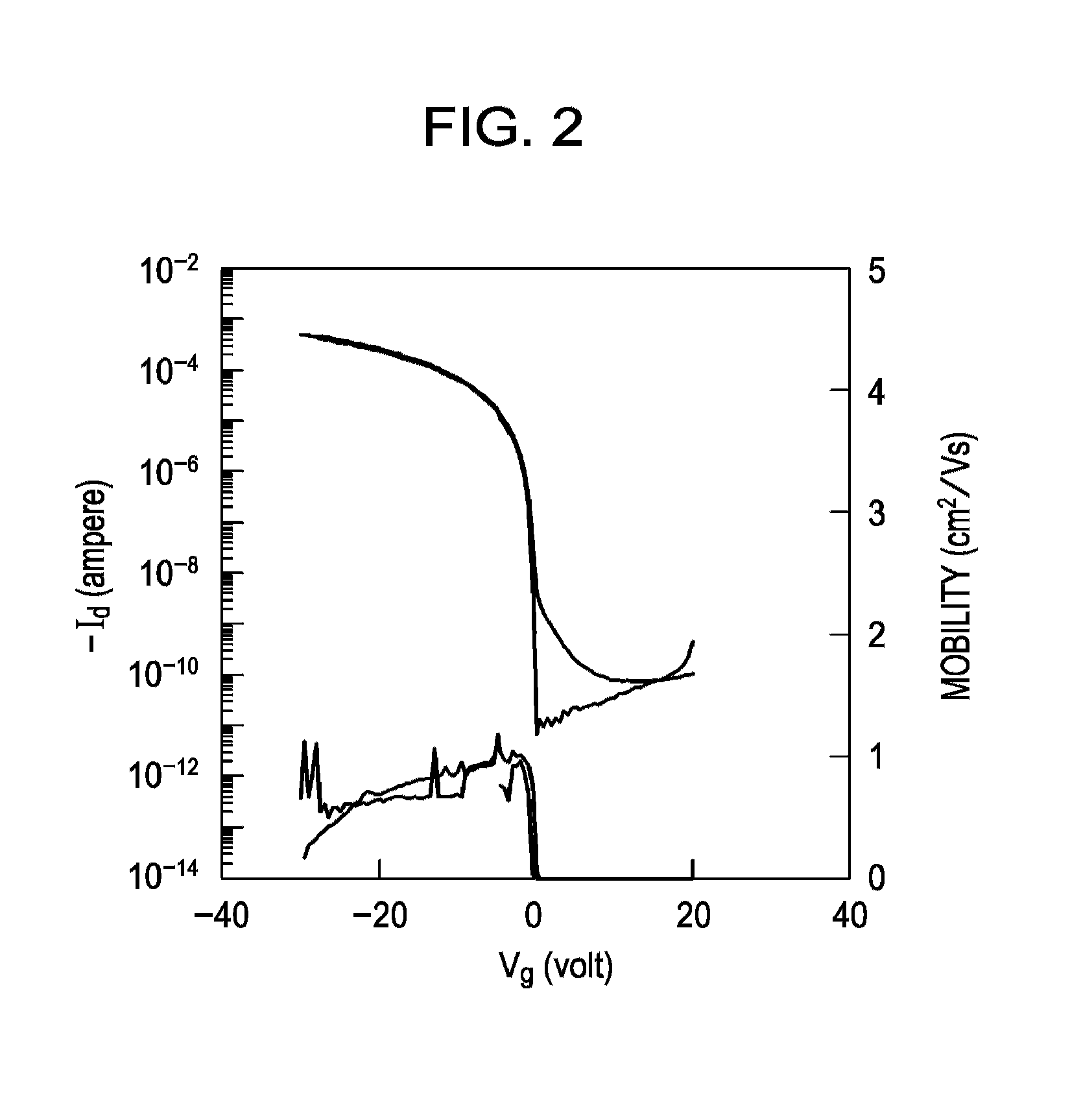
[0139]As in Example 1, a semiconductor device was fabricated, and as in Example 1, an evaluation sample was fabricated. The gate voltage dependence of the current-voltage curve between source / drain electrodes of the resulting sample was measured. The results thereof are shown in FIG. 4. As is evident from FIG. 4, current modulation occurs in response to the change in the gate electrode, thus confirming the characteristics of a transistor. Furthermore, as shown in FIG. 4, the mobility is 1 cm2 / Vs. The conditions are shown below.

[0140]Channel length (distance between source / drain electrodes): 50 μm

[0141...

example 3

[0143]Example 3 is also a modification of Example 1. In Example 3, an evaluation sample was fabricated as in Example 1 except that a thermal oxide film (SiO2 film with a thickness of 150 nm) was formed instead of forming an insulating film composed of PVP on the surface of the silicon semiconductor substrate.

[0144]Furthermore, as Comparative Example 3, an evaluation sample was fabricated in the same manner as that of Example 3 using a solution obtained by dissolving only PXX—(C2Ph)2 in tetralin.

[0145]The gate voltage dependence of the current-voltage curve between source / drain electrodes of the resulting sample of each of Example 3 and Comparative Example 3 was measured. The results thereof are shown in FIG. 5. As is evident from FIG. 5, current modulation occurs in response to the change in the gate electrode, thus confirming the characteristics of a transistor. In FIG. 5, “A” indicates the results of Example 3 and “B” indicates the results of Comparative Example 3. In the sample o...


PUM


Abstract

A method of manufacturing a semiconductor device including a gate electrode, a gate insulating layer, source / drain electrodes, and a channel-forming region that are disposed on a base is provided. The method includes the steps of forming a thin film by application of a mixed solution including a polymeric insulating material and a dioxaanthanthrene compound represented by structural formula (1) below; and subsequently drying the thin film to induce phase separation of the polymeric insulating material and the dioxaanthanthrene compound, thereby forming the gate insulating layer from the polymeric insulating material and the channel-forming region from the dioxaanthanthrene compound:wherein at least one of R3 and R9 represents a substituent other than hydrogen.

Description

BACKGROUND OF THE INVENTION[0001]1. Field of the Invention[0002]The present invention relates to a semiconductor device including a channel-forming region composed of a dioxaanthanthrene compound, a method of manufacturing the same, and a method of forming a multilayer semiconductor thin film including a semiconductor layer composed of a dioxaanthanthrene compound.[0003]2. Description of the Related Art[0004]In recent years, semiconductor devices including semiconductor layers composed of organic semiconductor materials have been receiving considerable attention. In such semiconductor devices, semiconductor layers can be formed by low-temperature coating in contrast to structures including semiconductor layers composed of inorganic materials. Therefore, such semiconductor devices are advantageous in that device area can be increased, and can be disposed on a flexible substrate that has low heat resistance, such as a plastic substrate. An increase in the range of functions and a redu...

Claims


Application Information

Patent Timeline
Patent Type & Authority Patents(United States)
IPC IPC(8): H01L51/40
CPCH01L51/0003H01L51/052H01L51/0558H01L51/0062H01L51/0516H01L51/0073H10K71/12H10K85/6574H10K10/471H10K10/484H10K85/649H10K10/468
Inventor KOBAYASHI, NORIHITOSASAKI, MARIOHE, TAKAHIRO
Owner SONY CORP
Why Eureka
Try Eureka