Pixelated capacitance controlled ESC

a capacitance control and capacitance technology, applied in the field of semiconductor manufacturing, can solve the problems of difficult to achieve the uniformity of etching across the surface of the substrate, difficult to achieve allowable cd variation across the substrate processed within the processing chamber, and difficult to achieve uniform radio frequency fields

Active Publication Date: 2016-10-18
APPLIED MATERIALS INC
View PDF44 Cites 146 Cited by
  • Summary
  • Abstract
  • Description
  • Claims
  • Application Information

AI Technical Summary

Problems solved by technology

Allowable CD variation across a substrate processed within a processing chamber is difficult to achieve due to chamber asymmetries such as chamber and substrate temperature, flow conductance, and RF fields.
In processes utilizing an electrostatic chuck, uniformity of etching across the surface of the substrate is challenging due to the non-homogeneous construction of the chuck below the substrate.
The non-homogeneous construction of the chuck leads to non-uniformity of the radio frequency (RF) fields which directly affect the etching across the surface of the substrate.
The structure of the electrostatic chuck can vary both laterally and azimuthally, uniformity of the RF field between the chuck and substrate is complicated and very difficult to obtain, resulting in local variability in the RF field across the chuck surface.
Thus, the local RF coupling variations result in non-uniformity of the processing results along the surface of the substrate.

Method used


Image

  • Pixelated capacitance controlled ESC
  • Pixelated capacitance controlled ESC
  • Pixelated capacitance controlled ESC

Examples


Embodiment Construction

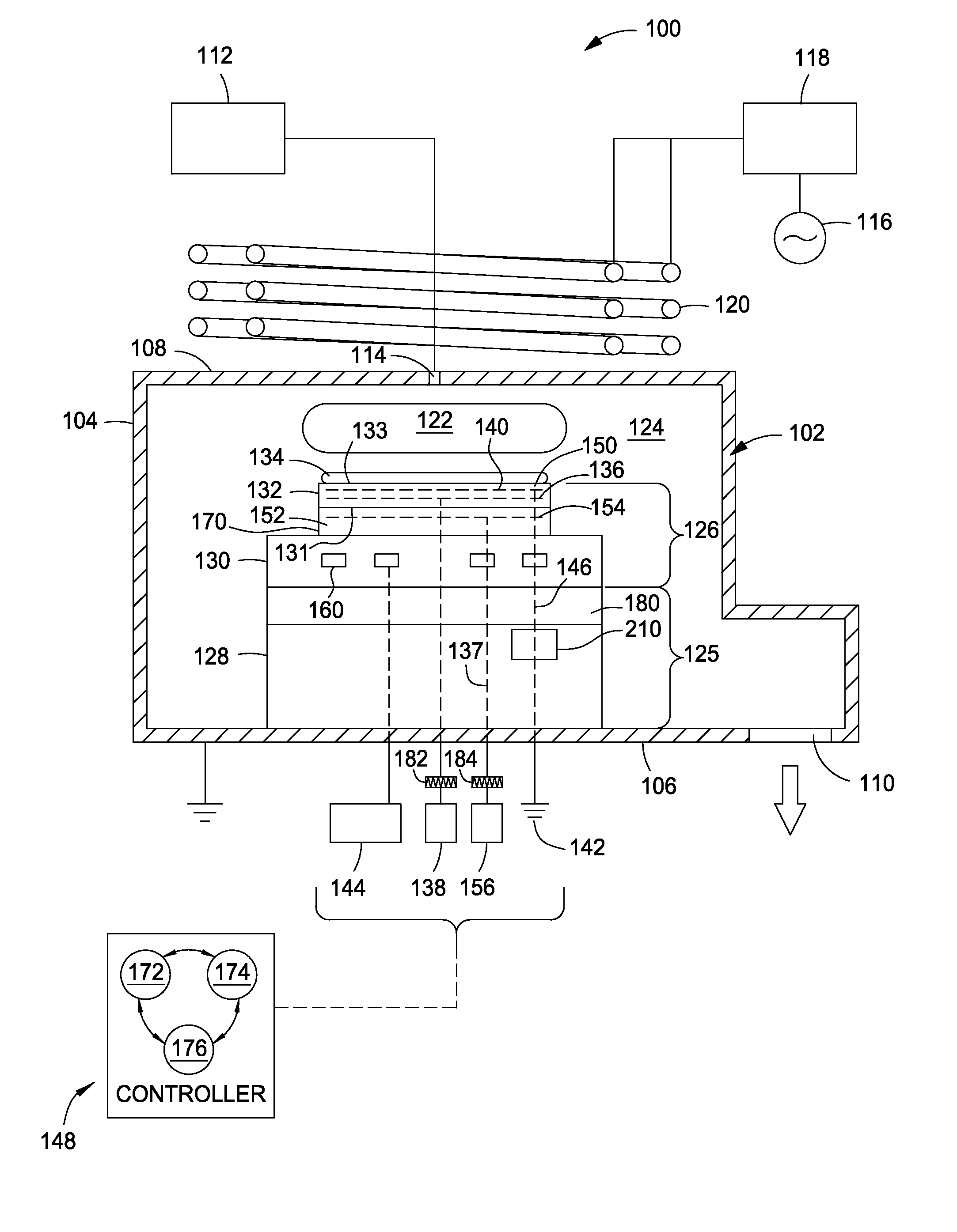
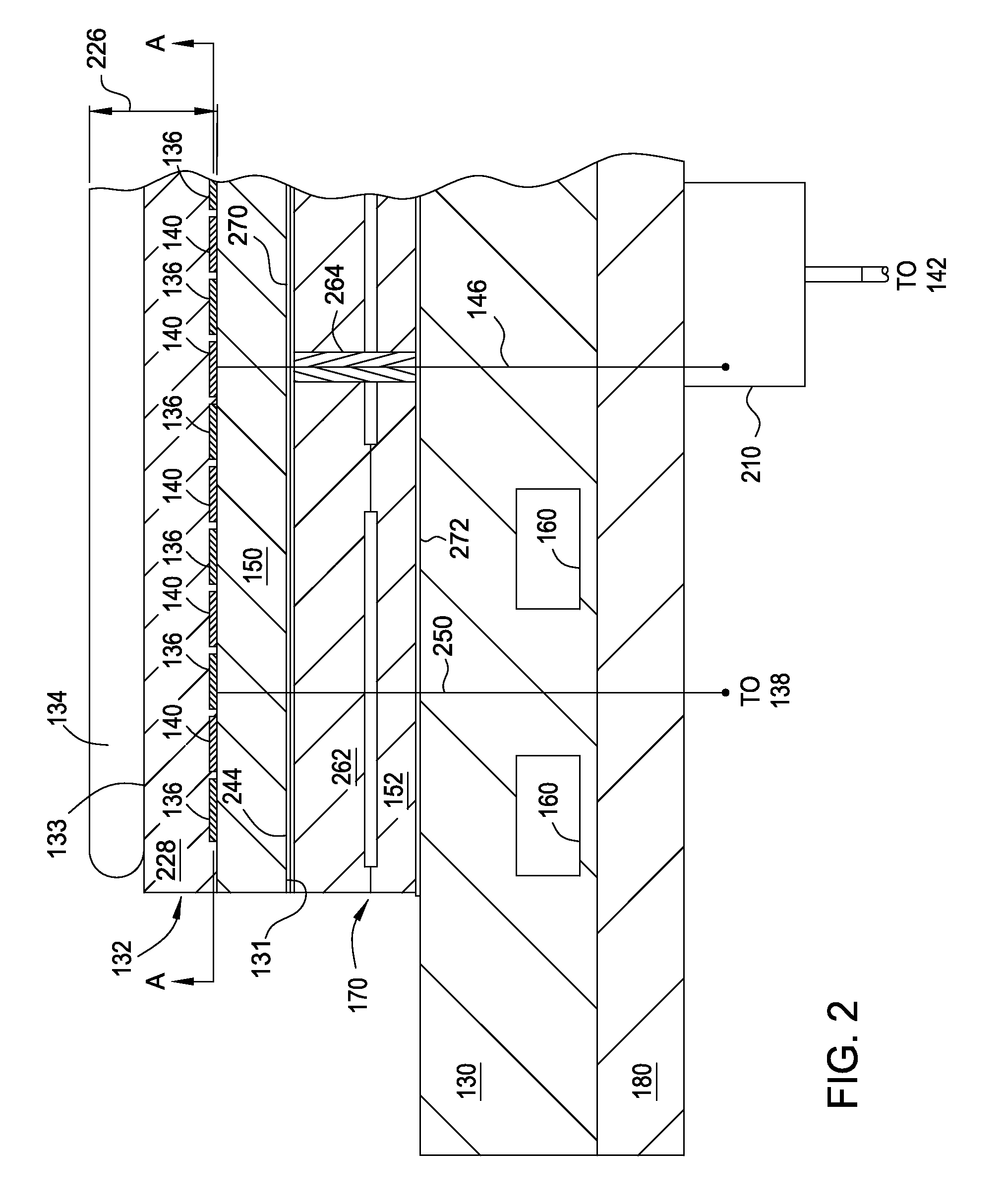
[0020]As the semiconductor industry is reducing the electronic feature sizes to sub-nm levels, the etch rate and CD uniformity requirements are also shrinking to Angstrom levels which is nearing atomic sizes. In such cases, substrate temperatures must either be very uniform, for example less than about 0.5° Celsius for nodes smaller than 20 nm, or tunable with a very fine resolution to tailor the process uniformity across substrates. However, for semiconductor technology nodes smaller than 10 nm, even temperature uniformity as low as 0.25° Celsius or less is not sufficient to maintain process uniformity. One factor effecting process uniformity is the dielectric depth of the chucking electrode within the puck of the electrostatic chuck. The dielectric depth is a distance between the top of the puck and the high voltage grid comprising the chucking electrode. The topography of the puck's substrate support surface and dielectric depth both significantly influence RF coupling of a subst...


PUM

PropertyMeasurementUnit
capacitanceaaaaaaaaaa
poweraaaaaaaaaa

Abstract

Implementations described herein provide a pixilated electrostatic chuck which enables both lateral and azimuthal tuning of the RF coupling between an electrostatic chuck and a substrate placed thereon. In one embodiment, the pixilated electrostatic chuck (ESC) may include a dielectric body having a workpiece support surface configured to accept a substrate thereon, one or more chucking electrodes disposed in the pixilated ESC, and a plurality of pixel electrodes. The plurality of pixel electrodes are switchable between a floating state and a grounded state, having variable capacitance to ground, or both. The pixel electrodes and the chucking electrodes form a circuit operable to electrostatically chuck the substrate to the workpiece support surface.

Description

CROSS-REFERENCE TO RELATED APPLICATIONS[0001]This application claims benefit of U.S. Provisional Application Ser. No. 61 / 984,519, filed Mar. 5, 2014, of which is incorporated by reference in its entirety.BACKGROUND[0002]1. Field[0003]Implementations described herein generally relate to semiconductor manufacturing and more particularly to an electrostatic chuck and a method of using the same.[0004]2. Description of the Related Art[0005]As the feature size of the device patterns get smaller, the critical dimension (CD) requirements of these features become a more important criterion for stable and repeatable device performance. Allowable CD variation across a substrate processed within a processing chamber is difficult to achieve due to chamber asymmetries such as chamber and substrate temperature, flow conductance, and RF fields.[0006]In processes utilizing an electrostatic chuck, uniformity of etching across the surface of the substrate is challenging due to the non-homogeneous cons...

Claims


Application Information

Patent Timeline
Patent Type & Authority Patents(United States)
IPC IPC(8): H01L21/683H01L21/3213H01L21/311H01L21/3065H01L21/265H01L21/02H01J37/32C23C16/00H04N7/18H01T23/00H01L21/285G06K9/00
CPCH01L21/28556C23C16/00H01J37/32715H01L21/0228H01L21/0262H01L21/02252H01L21/02274H01L21/265H01L21/3065H01L21/31116H01L21/31138H01L21/32136H01L21/6833H04N7/181H04N7/188G06K2009/00738B23Q3/15H02N13/00H01J37/32697G06V20/44H01L21/67103H01L27/1255H01J2237/334H01L21/67063H01L29/93
Inventor SADJADI, REZABOYD, JR., WENDELL GLENPARKHE, VIJAY D.NOGINOV, MAXIM MIKHAILOVICH
Owner APPLIED MATERIALS INC
Why Eureka
Try Eureka