Reverse conducting semiconductor device
a semiconductor and reverse conducting technology, applied in semiconductor devices, diodes, electrical devices, etc., can solve the problems of changing the contact area between the barrier metal and the high-concentration anode layer, and the difficulty of connecting the anode layer and the emitter electrode by a contact electrode formed of aluminum,
- Summary
- Abstract
- Description
- Claims
- Application Information
AI Technical Summary
Benefits of technology
Problems solved by technology
Method used
Image
Examples
first embodiment
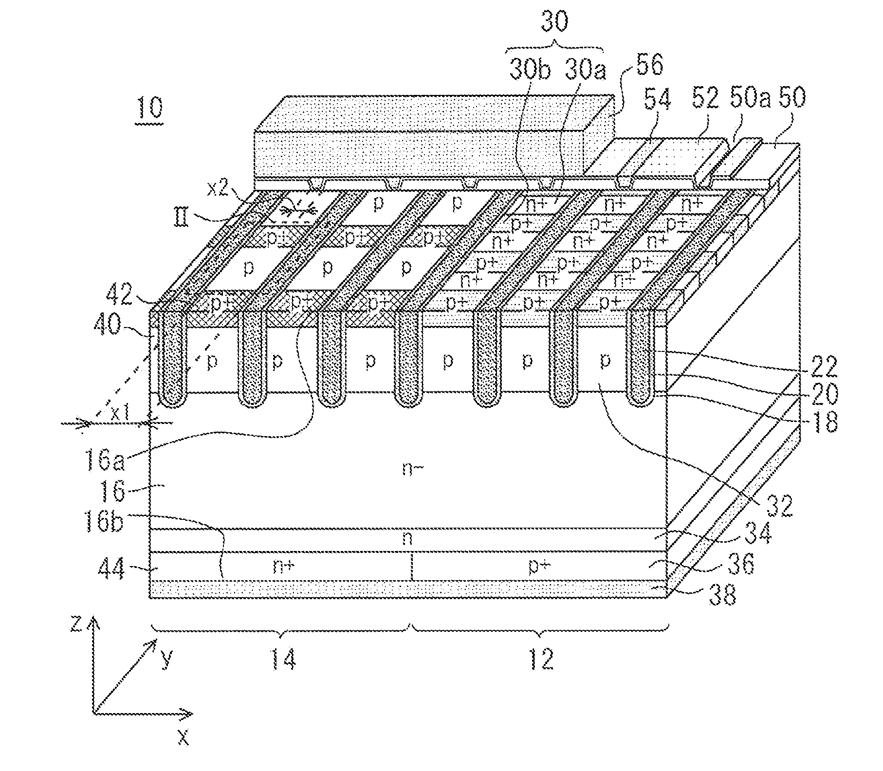
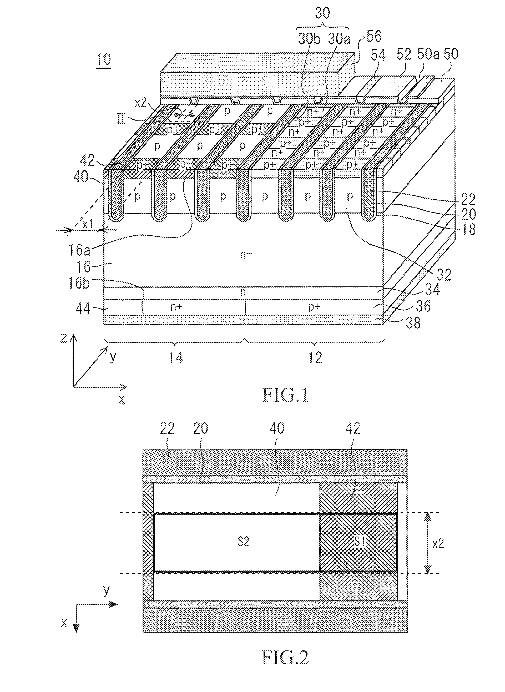
[0018]FIG. 1 is a perspective view of a reverse conducting semiconductor device 10 according to a first embodiment of the present invention. The reverse conducting semiconductor device 10 has a transistor 12 and a diode 14 formed horizontally adjacent to the transistor 12. The transistor 12 and the diode 14 are formed on a semiconductor substrate 16. The semiconductor substrate 16 is a first conduction type (n-type) of substrate having a first major surface 16a and a second major surface 16b.
[0019]A plurality of trenches 18 in stripe form are provided in the first major surface 16a. A gate oxide film 20 is formed on inner wall surfaces of the trenches 18. The trenches 18 have gate electrodes 22 formed therein, filling the trenches 18 and bordering the gate oxide film 20. The gate electrodes 22 are formed of polysilicon for example. The trenches 18, the gate oxide film 20 and the gate electrodes 22 are formed both in the transistor 12 and in the diode 14.
[0020]The transistor 12 has ...
second embodiment
[0038]FIG. 6 is a perspective view of a reverse conducting semiconductor device according to a second embodiment of the present invention. The reverse conducting semiconductor device according to the second embodiment have a number of commonalities with the first embodiment and will therefore be described with respect to points of difference from the first embodiment. Segments of a high-concentration anode layer 100 are disposed in a staggered pattern as viewed in plan. That is, the high-concentration anode layer 100 is formed in zigzag such that each segment of the high-concentration anode layer does not border any of the other segments through the gate oxide film 20 and the gate electrode 22.
[0039]Disposing segments of a high-concentration anode layer 100 in a staggered pattern as viewed in plan enables uniformization of the current distribution in the diode 14. Prevention of a local increase in temperature of the diode 14 at a particular position can be achieved by uniformizing t...
PUM
 Abstract
Description
Claims
Application Information


