Semiconductor device
a technology of semiconductors and devices, applied in the direction of semiconductor devices, electrical equipment, transistors, etc., can solve the problems of electrical characteristics that vary among transistors, and achieve the effect of improving reliability and less power consumption
- Summary
- Abstract
- Description
- Claims
- Application Information
AI Technical Summary
Benefits of technology
Problems solved by technology
Method used
Image

Examples
embodiment 1
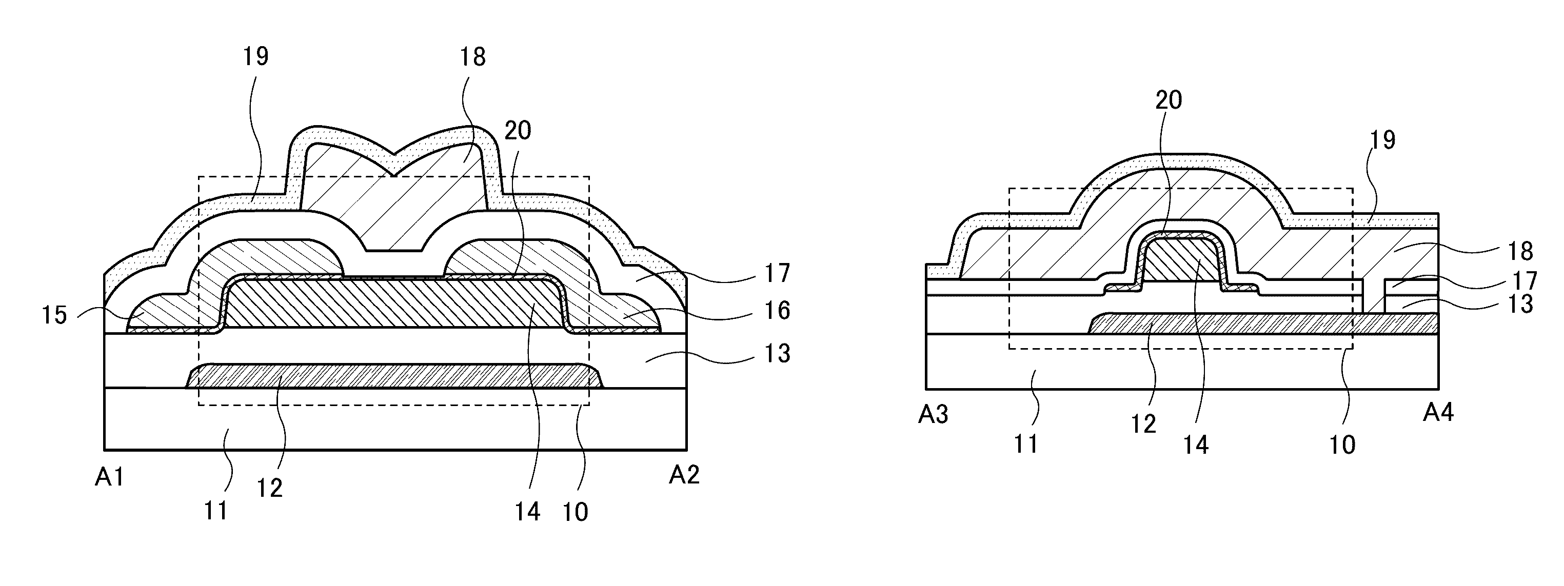
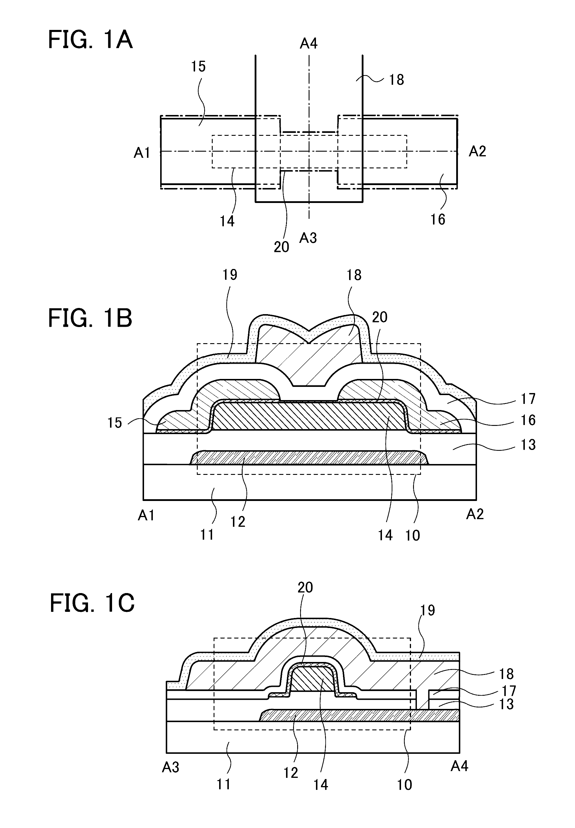
[0109]In this embodiment, a semiconductor device of one embodiment of the present invention and a method for manufacturing the semiconductor device are described with reference to drawings. A transistor 10 described in this embodiment has a dual-gate structure.
[0110]FIGS. 1A to 1C are a top view and cross-sectional views of the transistor 10 included in a semiconductor device. FIG. 1A is a top view of the transistor 10, FIG. 1B is a cross-sectional view taken along dashed-dotted line A1-A2 in FIG. 1A, and FIG. 1C is a cross-sectional view taken along dashed-dotted line A3-A4 in FIG. 1A. In FIGS. 1A to 1C, some components are enlarged, reduced in size, or omitted for easy understanding. In some cases, the direction of the dashed-dotted line A1-A2 is referred to as a channel length direction, and the direction of the dashed-dotted line A3-A4 is referred to as a channel width direction.
[0111]The transistor 10 illustrated in FIGS. 1A to 1C includes a conductive film 12 over a substrate ...
modification example 2
[0240]A modification example of the transistor 10 described in this embodiment is described with reference to FIGS. 7A to 7C. In this modification example, a transistor in which an oxide semiconductor film is provided between a gate insulating film and a pair of electrodes is described.
[0241]FIGS. 7A to 7C are a top view and cross-sectional views of a transistor 10e included in a semiconductor device of one embodiment of the present invention. FIG. 7A is a top view, FIG. 7B is a schematic cross-sectional view taken along dot-dashed line A1-A2 in FIG. 7A, and FIG. 7C is a schematic cross-sectional view taken along dot-dashed line A3-A4 in FIG. 7A. In FIGS. 7A to 7C, some components are enlarged, reduced in size, or omitted for easy understanding.
[0242]The transistor 10e illustrated in FIG. 7A includes the conductive film 12 over the substrate 11, the base insulating film 13 over the substrate 11 and the conductive film 12, the oxide semiconductor film 26 over the base insulating film...
embodiment 2
[0280]In this embodiment, a transistor having a structure different from the structures of the transistors described in Embodiment 1 will be described.
[0281]FIGS. 13A to 13C are a top view and cross-sectional views of the transistor 50 included in a semiconductor device. FIG. 13A is a top view of the transistor 50, FIG. 13B is a cross-sectional view taken along dashed-dotted line B1-B2 in FIG. 13A, and FIG. 13C is a cross-sectional view taken along dashed-dotted line B3-B4 in FIG. 13A. In FIGS. 13A to 13C, some components are enlarged, reduced in size, or omitted for easy understanding. In some cases, the direction of the dashed-dotted line B1-B2 is referred to as a channel length direction, and the direction of the dashed-dotted line B3-B4 is referred to as a channel width direction.
[0282]The transistor 50 illustrated in FIGS. 13A to 13C includes the conductive film 12 over the substrate 11, the base insulating film 13 over the substrate 11 and the conductive film 12, the oxide sem...
PUM
 Abstract
Description
Claims
Application Information
 - R&D
- Intellectual Property
- Life Sciences
- Materials
- Tech Scout
- Unparalleled Data Quality
- Higher Quality Content
- 60% Fewer Hallucinations
Browse by: Latest US Patents, China's latest patents, Technical Efficacy Thesaurus, Application Domain, Technology Topic, Popular Technical Reports.
© 2025 PatSnap. All rights reserved.Legal|Privacy policy|Modern Slavery Act Transparency Statement|Sitemap|About US| Contact US: help@patsnap.com