
Semiconductor module cooler

a technology of semiconductor modules and coolers, applied in the direction of semiconductor devices, semiconductor/solid-state device details, electrical apparatus, etc., can solve the problem of large amount of heat generated by power semiconductor elements, and achieve the effect of reducing the temperature difference between the semiconductor elements generating heat and sufficient output curren

Active Publication Date: 2016-11-22
FUJI ELECTRIC CO LTD
View PDF35 Cites 5 Cited by
  • Summary
  • Abstract
  • Description
  • Claims
  • Application Information

AI Technical Summary

Benefits of technology

This design allows for uniform cooling of semiconductor elements, reducing temperature differences and ensuring sufficient output current by promoting even flow of the cooling medium across the cooling fins, thereby enhancing the cooling efficiency and output performance.

Problems solved by technology

In particular, with a reduction in the size of the power semiconductor element or an increase in the output from the power semiconductor element, a very large amount of heat is generated from the power semiconductor element.

Method used


Image

  • Semiconductor module cooler
  • Semiconductor module cooler
  • Semiconductor module cooler

Examples


Embodiment Construction

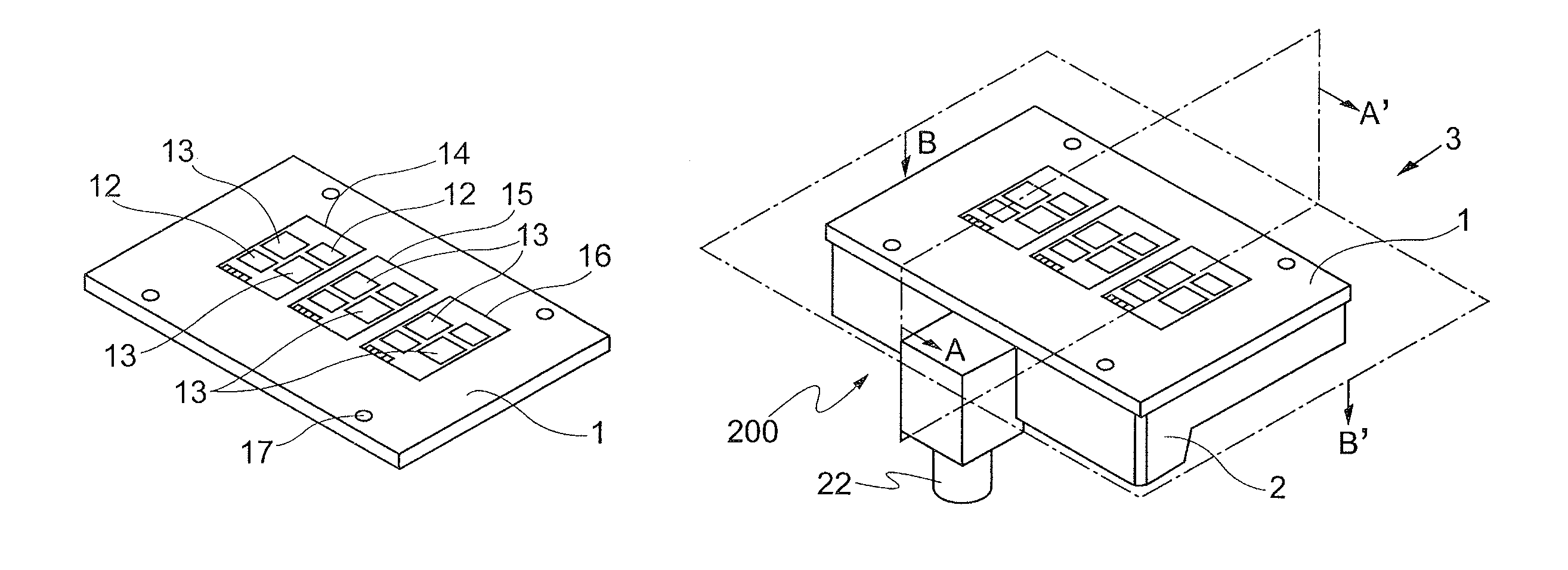
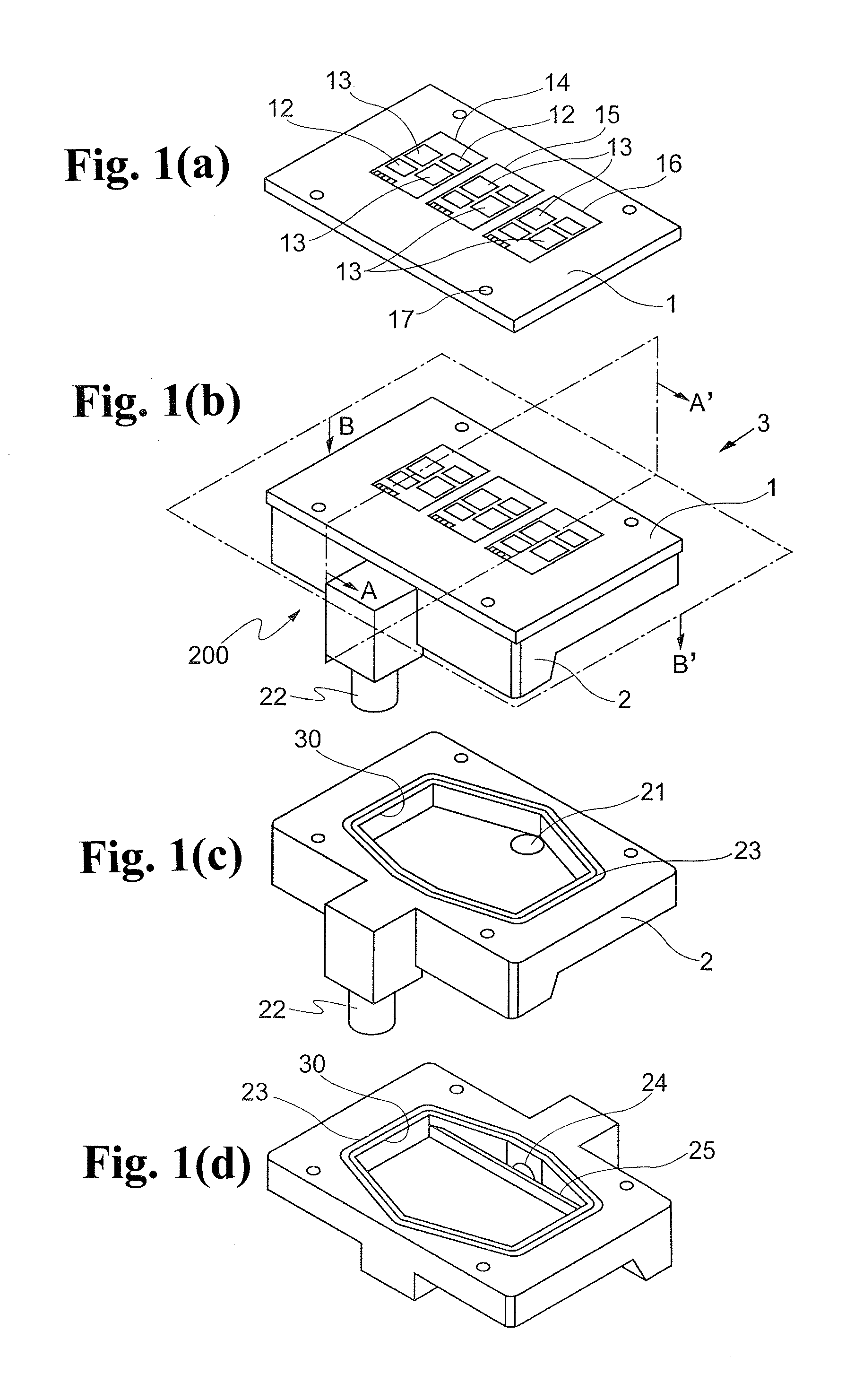
[0051]FIGS. 1(a)-1(d) are diagrams illustrating the outward appearance and internal structure of a semiconductor module cooler according to the invention. FIG. 1(b) illustrates the outward appearance of a semiconductor module cooler 3. FIG. 1(a) illustrates a heat sink 1 according to the invention and semiconductor circuits (14, 15, and 16) attached to the heat sink 1. Here, an example of the semiconductor circuit is an IGBT (Insulated Gate Bipolar Transistor) module. FIG. 1(c) illustrates a cooling medium jacket (water jacket) 2 according to the invention. FIG. 1(d) is a diagram illustrating a cooling medium introduction port of the cooling medium jacket (water jacket) 2 according to the invention.

[0052]Here, the semiconductor circuits 14, 15, and 16 are a circuit for a W phase, a circuit for a V phase, and a circuit for a U phase forming a three-phase inverter. As illustrated in FIG. 1(a), in the semiconductor circuit 14 serving as the circuit for a W phase, an IGBT element 13 ser...


PUM


Abstract

A semiconductor module cooler supplies a cooling medium to a cooling medium jacket from outside to cool a plurality of semiconductor elements thermally connected to the cooling medium jacket through a heat sink. The cooling medium jacket has a cooling fin cooling room including an opening for inserting cooling fins, and cooling the cooling fins; a cooling medium introduction port to introduce the cooling medium; a cooling medium diffusion room to diffuse and supply the cooling medium to the cooling fin cooling room; a cooling medium diffusion wall provided in the cooling medium diffusion room in which the cooling medium diffused by the cooling medium diffusion room flows over to be introduced to the cooling fin cooling room side; a cooling medium discharge port discharging the cooling medium to the outside; and a cooling medium convergence room provided between the cooling fin cooling room and the cooling medium discharge port.

Description

RELATED APPLICATIONS[0001]The present application is National Phase of International Application No. PCT / JP2012 / 003141 filed May 14, 2012, and claims priority from Japanese Applications No. 2011-109215 filed May 16, 2011 and No. 2011-244350 filed Nov. 8, 2011.TECHNICAL FIELD[0002]The present invention relates to a semiconductor module cooler, and more particularly, to a semiconductor module cooler in which heat dissipation fins are integrally formed on a rear surface of a heat sink to which an insulating substrate having a plurality of semiconductor elements arranged thereon is bonded and a cooling medium flows between the heat dissipation fins to dissipate heat generated from the semiconductor elements.BACKGROUND ART[0003]Semiconductor modules are widely used in power conversion devices which are generally used in, for example, hybrid vehicles or electric vehicles. A semiconductor module forming a control device for saving energy includes a power semiconductor element for controlli...

Claims


Application Information

Patent Timeline
Patent Type & Authority Patents(United States)
IPC IPC(8): H01L23/473H01L25/07H01L23/00
CPCH01L23/473H01L24/32H01L25/072H01L2224/32225H01L2924/1203H01L2924/1305H01L2924/13055H01L2924/00
Inventor NAGAUNE, FUMIO
Owner FUJI ELECTRIC CO LTD
Learn More