Double-lens structures and fabrication methods thereof

a technology of double lenses and microlens arrays, applied in the field of microlens arrays, can solve the problems of inability to improve the sensitivity of solid-state imaging sensors and large amount of incident light, and achieve the effect of improving the condensing efficiency of microlens arrays and enhancing the sensitivity of solid-state image sensors

Active Publication Date: 2016-12-06
VISERA TECH CO LTD
View PDF16 Cites 0 Cited by
  • Summary
  • Abstract
  • Description
  • Claims
  • Application Information

AI Technical Summary

Benefits of technology

[0007]According to embodiments of the disclosure, a double-lens structure and a method for fabricating the same are provided. The double-lens structure is disposed over a solid-state image sensor and used as a microlens array for the solid-state image sensor to improve the condensing efficiency of the microlens array. The sensitivity of the solid-state image sensor is thereby enhanced.

Problems solved by technology

However, a large amount of incident light is not directed onto the photo-sensors.
The sensitivity of solid-state imaging sensors cannot be improved due to lost light.

Method used


Image

  • Double-lens structures and fabrication methods thereof
  • Double-lens structures and fabrication methods thereof
  • Double-lens structures and fabrication methods thereof

Examples


Embodiment Construction

[0017]The following description is of the contemplated mode of carrying out the disclosure. This description is made for the purpose of illustrating the general principles of the disclosure and should not be taken in a limiting sense. The scope of the disclosure is best determined by reference to the appended claims.

[0018]In some embodiments of the disclosure, a double-lens structure is used as a microlens array and disposed over a solid-state image sensor to improve the condensing efficiency of the microlens array. Therefore, the sensitivity of the solid-state image sensor is also enhanced.

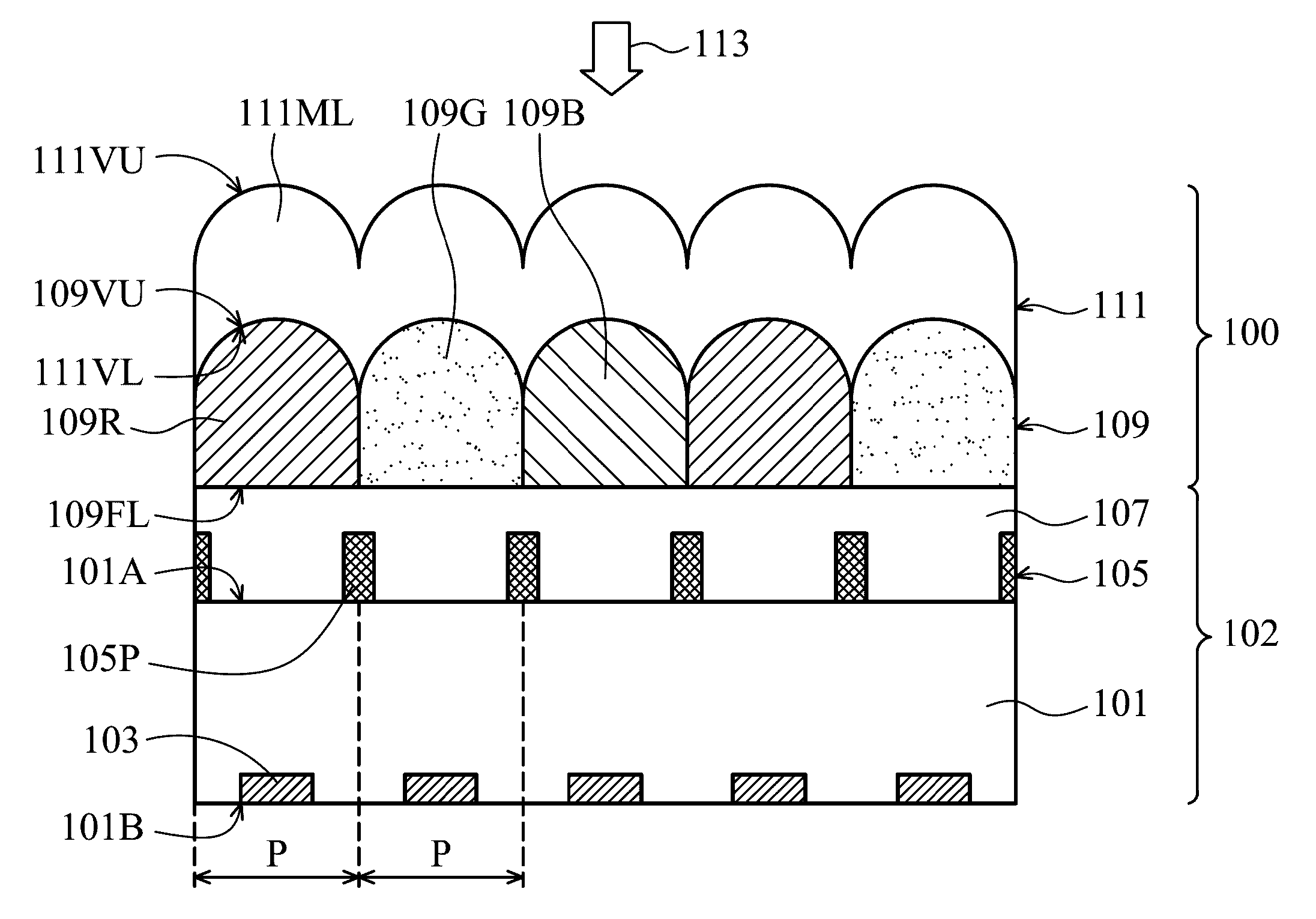
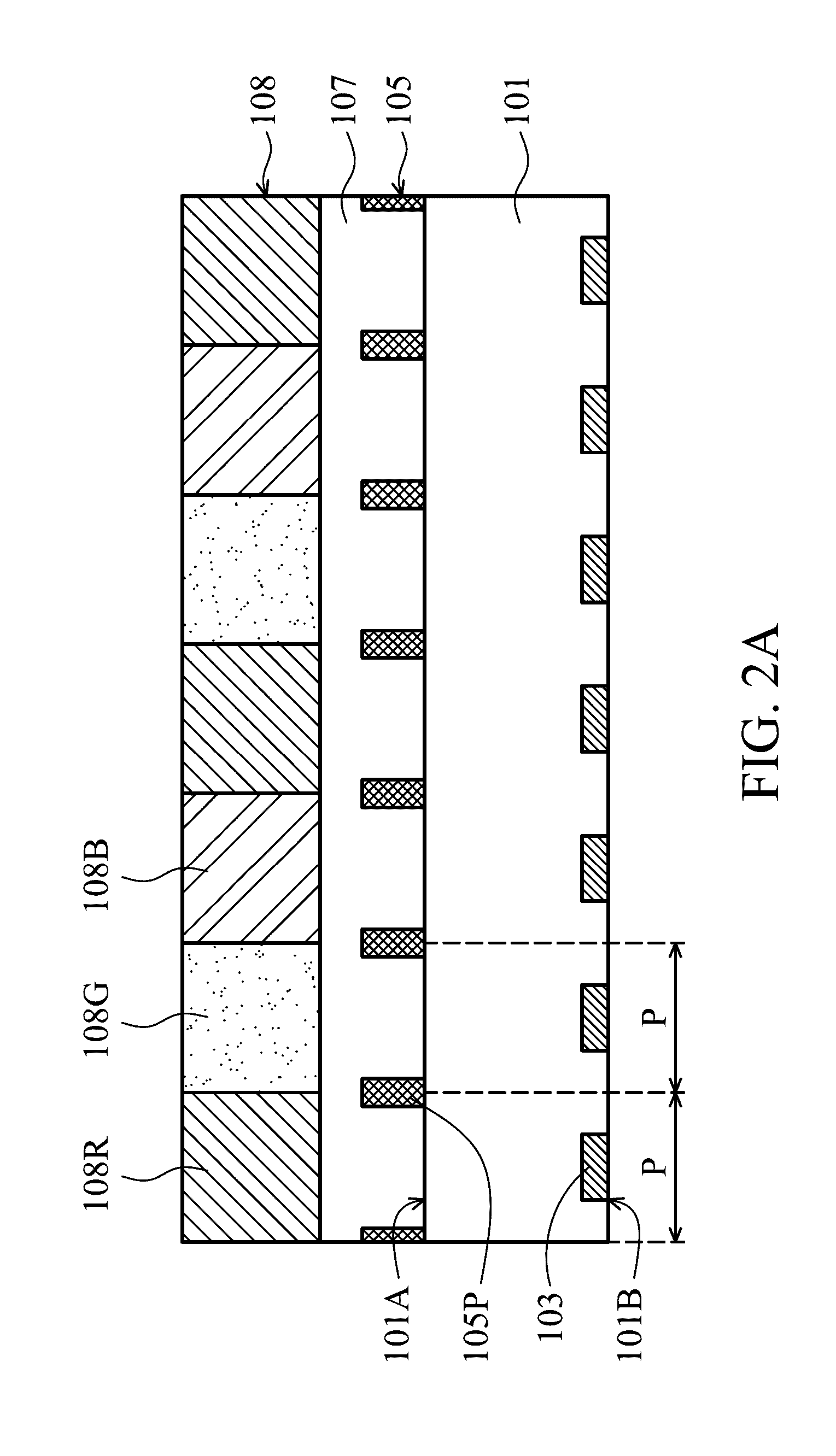
[0019]Referring to FIG. 1, a cross section of a portion of a double-lens structure 100 disposed over a solid-state image sensor 102 according to some embodiments is shown. The solid-state image sensor 102 includes a substrate 101, for example, a semiconductor substrate, having a front side surface 101A and a back side surface 101B. The semiconductor substrate may be a wafer or a chip. The solid-s...


PUM


Abstract

A double-lens structure and a method for fabricating the same are provided. The double-lens structure includes a first lens structure formed of a color filter layer having a first refractive index and a second lens structure formed of a micro-lens material layer having a second refractive index and disposed on the first lens structure. The first refractive index of the color filter layer is different from the second refractive index of the micro-lens material layer. An incident light enters the second lens structure and then passes through the first lens structure. Further, a method for fabricating the double-lens structure is also provided.

Description

BACKGROUND[0001]Field of the Invention[0002]The invention relates to a microlens array and more particularly to a microlens array having a double-lens structure for use in a solid-state image sensor, and a method for fabricating the same.[0003]Description of the Related Art[0004]Recently, solid-state imaging sensors have been developed and are widely used in various image-capturing apparatuses, for example video cameras, digital cameras, minicam adapted personal computers, minicam adapted mobile phones, and so forth. Image sensors absorb incident radiation of a particular wavelength, such as visible light, UV light, IR light, or the like and generate an electrical signal corresponding to the absorbed radiation. There are a number of different types of semiconductor-based image sensors, for example charge-coupled device (CCD) image sensors or complementary metal-oxide semiconductor (CMOS) image sensors.[0005]A solid-state imaging sensor typically consists of an array of pixels contai...

Claims


Application Information

Patent Timeline
Patent Type & Authority Patents(United States)
IPC IPC(8): G02B27/10G02B3/00H01L31/0232G02B5/20
CPCG02B3/0068G02B3/0012G02B5/201C09K13/00
Inventor WU, HAN-LINHSIAO, YU-KUNCHENG, YUEH-CHING
Owner VISERA TECH CO LTD
Why Eureka
Try Eureka