Solid-state imaging device

a solid-state imaging and imaging device technology, applied in the direction of semiconductor devices, basic electric elements, electrical apparatus, etc., can solve the problems of deteriorating condensing efficiency of light guides, and achieve the effect of improving condensing efficiency and reducing reflection

Inactive Publication Date: 2011-04-07
CANON KK
View PDF5 Cites 5 Cited by
  • Summary
  • Abstract
  • Description
  • Claims
  • Application Information

AI Technical Summary

Benefits of technology

[0008]In view of the above problem, it is an object of the present invention to provide a solid-state imaging device capable of making reduction in reflection at the interface between the light guide and the incident unit consistent with improvement in condensing efficiency by the light guide.
[0010]The present invention can realize a solid-state imaging device capable of making reduction in reflection at the interface between the light guide and the incident unit consistent with improvement in condensing efficiency by the light guide.

Problems solved by technology

However, if the refractive index of the high refractive index unit is high, reflection at the interface between the light guide and the incident unit is increased, and the condensing efficiency by the light guide is deteriorated.

Method used


Image

  • Solid-state imaging device
  • Solid-state imaging device
  • Solid-state imaging device

Examples


embodiment 1

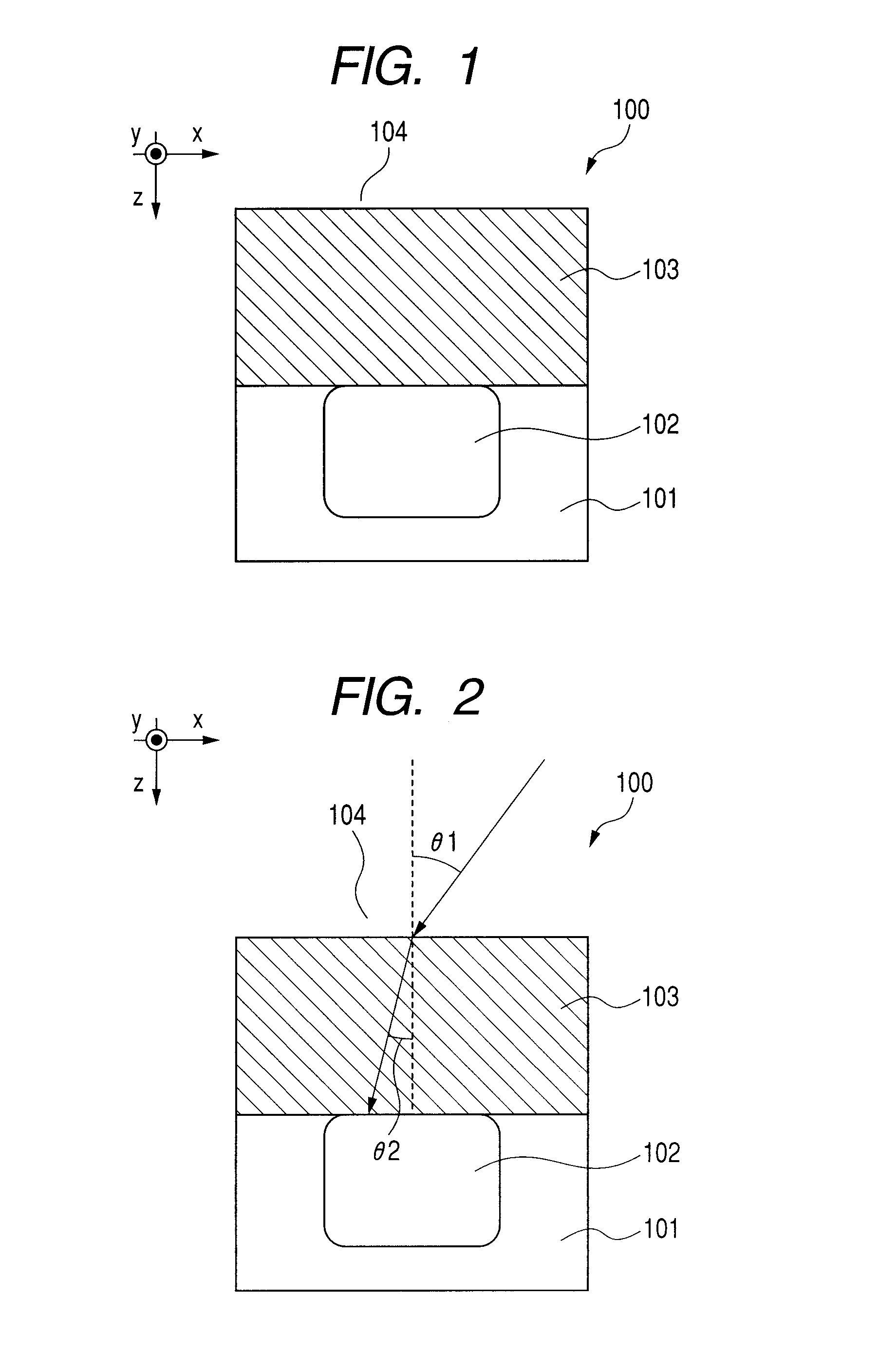
[0038]An example of a solid-state imaging device according to an embodiment 1 of the present invention will be described using FIG. 1. FIG. 1 illustrates a schematic sectional view of a pixel unit 100 of the solid-state imaging device. The solid-state imaging device includes a substrate internally containing a photoelectric conversion unit of this embodiment, and a condensing unit provided on an optical incident side of the substrate. Incident light from the optical incident side is guided through the condensing unit to the photoelectric conversion unit. The solid-state imaging device of this embodiment includes a plurality of pixel units 100 arranged in a matrix manner. The pixel unit 100 includes a silicon substrate 101 and a photoelectric conversion unit 102 arranged inside of the silicon substrate 101. In the pixel unit 100, a condensing unit 103 is formed above the silicon substrate 101. Hereinafter, a region above the condensing unit 103 is referred to as an optical incident u...

embodiment 2

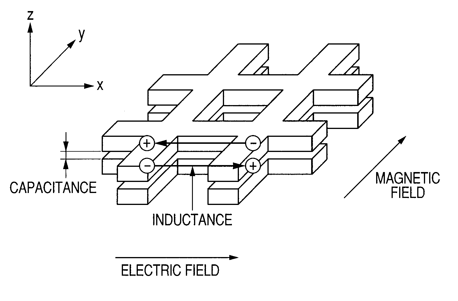
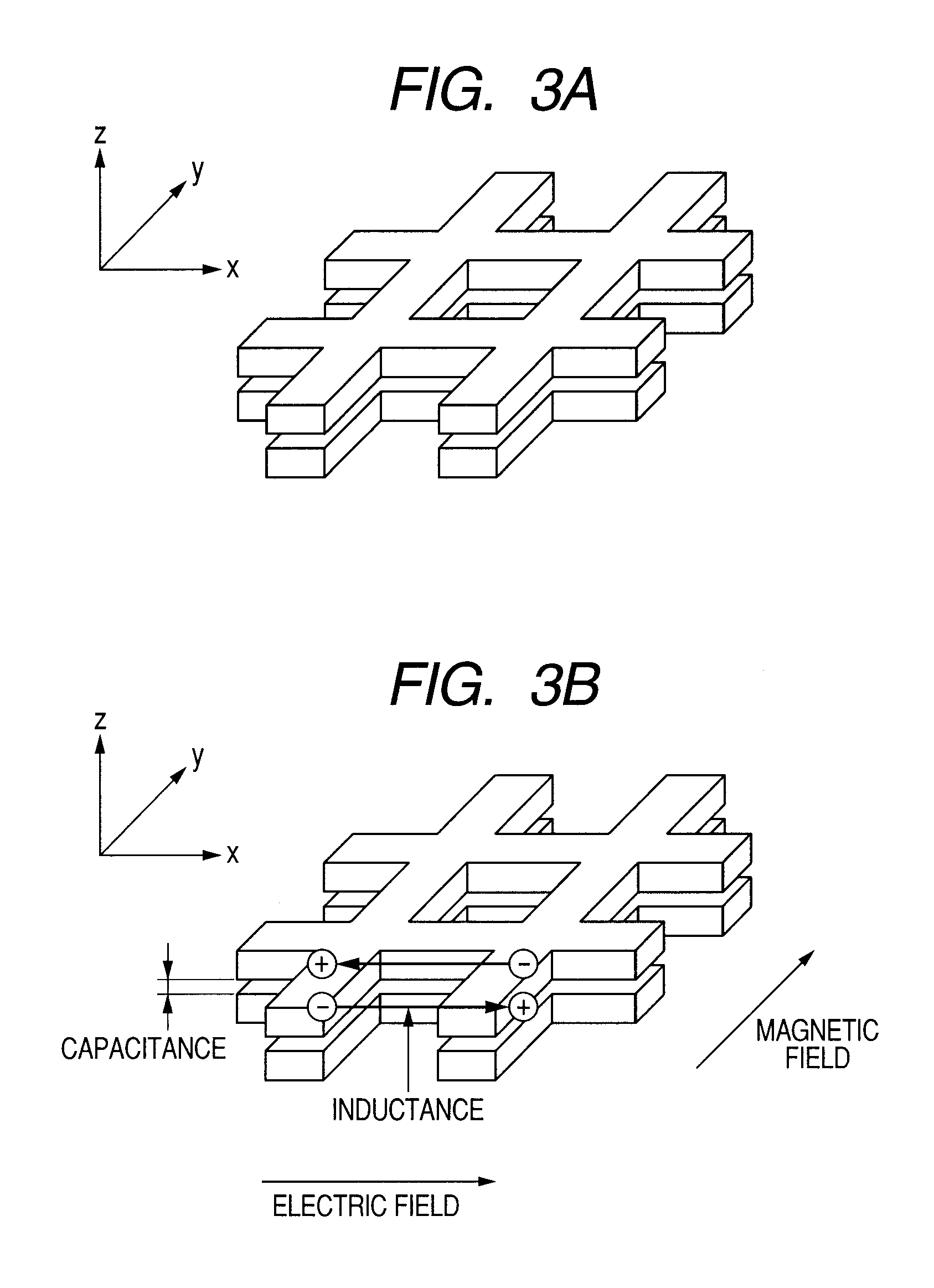
[0057]A solid-state imaging device according to an embodiment 2 will be described using FIGS. 8A and 8B. This embodiment is different from the embodiment 1 in the following configuration. That is, in this embodiment, the specific permittivity ∈ and the specific permeability μ of the condensing unit 113 satisfy the expression of condition, |N1|102 is N3, the value of √∈ / √μ is changed so as to hold √∈ / √μ=N1 at the optical incident side and √∈ / √μ=N3 at the photoelectric conversion unit side.

[0058]As described above, the smaller the reflectivity on the boundary interface is, the closer to one the impedance ratio between two media contact with each other at the boundary becomes. Accordingly, if √∈ / √μ=N3 holds, the reflection between the condensing unit 113 and the photoelectric conversion unit 102 can be suppressed. Further, the absolute value √∈×√μ| of the refractive index of the condensing unit 113 has a value higher than the absolute value |N1| of the refractive index of the optical i...

embodiment 3

[0063]An example of a configuration of a solid-state imaging device according to an embodiment 3 will be described using FIGS. 9A and 9B. This embodiment is different from the embodiment 1 in the following configuration. That is, this embodiment includes a structure where a barrier unit 105 is arranged around the condensing unit 103, as illustrated in FIG. 9A. Further, provided that the specific permittivity of the barrier unit 105 is ∈2 and the specific permeability is μ2, the barrier unit 105 is configured so as to satisfy the following relationship (Expression 3).

|√∈2×√μ2|<|√∈×√μ|  (Expression 3)

[0064]If the absolute value |√∈×√μ| of the refractive index of the condensing unit 103 is larger than the absolute value |√∈2×√μ2| of the refractive index of the barrier unit 105, the light incident from the optical incident unit 104 can be condensed in the condensing unit 103 and guided to the photoelectric conversion unit 102. Accordingly, light leaking to adjacent pixels can be reduced...


PUM


Abstract

A solid-state imaging device capable of making reduction in reflection at the interface between a light guide and an incident unit consistent with improvement in condensing efficiency by the light guide is provided. The solid-state imaging device includes a substrate internally including a photoelectric conversion unit, and a condensing unit provided on an optical incident side of the substrate. A configuration satisfying relationships of |N1|<|√∈×√μ| and 0.63<N1 / (√∈ / √μ)<1.58 on an end face of the optical incident side of the condensing unit is adopted. Here, N1 is a refractive index of a medium forming a region of the optical incident side of the condensing unit, and ∈ is a specific permittivity of a medium forming the condensing unit, and μ is a specific permeability of the medium forming the condensing unit.

Description

BACKGROUND OF THE INVENTION[0001]1. Field of the Invention[0002]The present invention relates to a solid-state imaging device, and particularly to a solid-state imaging device used for a digital video camera and a digital still camera.[0003]2. Description of the Related Art[0004]In a solid-state imaging device used for a digital still camera or the like, there has been a tendency that the number of pixels is increased, while size of a pixel is reduced. Accordingly, the area of a photoelectric conversion unit is reduced, thereby reducing light receiving sensitivity. Further, the aspect ratio (depth / width) of a pixel structure is increased. The F-number of an on-chip lens is also increased. This reduces condensing efficiency, and light leaks to adjacent pixels, thereby causing crosstalk.[0005]Conventionally, a solid-state imaging device including light guides as described in Japanese Patent Application Laid-Open No. H06-224398 has been proposed as a solution to these problems. The sol...

Claims


Application Information

Patent Timeline
Patent Type & Authority Applications(United States)
IPC IPC(8): H01L31/0232
CPCH01L27/14685H01L27/14625
Inventor NUMATA, AIHIKOTAKAGI, AKINARI
Owner CANON KK
Why Eureka
Try Eureka