
Substrate for optics and light emitting device

a technology of applied in the field of substrates for optics and light emitting devices, can solve the problems of difficult practical use and abrupt color shift, and achieve the effect of suppressing color shift and glare caused by diffraction of light and improving light extraction efficiency

Inactive Publication Date: 2017-01-10
ASAHI KASEI E-MATERIALS CORPORATION
View PDF31 Cites 0 Cited by
  • Summary
  • Abstract
  • Description
  • Claims
  • Application Information

AI Technical Summary

Benefits of technology

[0047]According to the present invention, it is possible to provide the substrate for optics and light emitting device for improving light extraction efficiency, and enabling the color shift and glare caused by diffraction of light to be suppressed.

Problems solved by technology

Among the conventional techniques, in introducing the periodical grid structure of metal near the light emitting portion and extracting light from the light emitting device using surface plasmon resonance, it is necessary to provide a substantially uniform periodical grid structure over the entire surface of the device, and since the periodicity is the size of diffracting visible light, there is a problem of developing an abrupt color shift caused by diffraction of light when the observation direction is varied.
The above-mentioned color shift and glare is the fatal problems as a display or light emitting device for illumination, and even when light extraction efficiency is improved as the entire device, it is hard to adopt as practical use.
Thus, in the case of using the diffraction structure, light extraction efficiency and light-emitting characteristics of the color shift and glare are mutually contradictory.

Method used

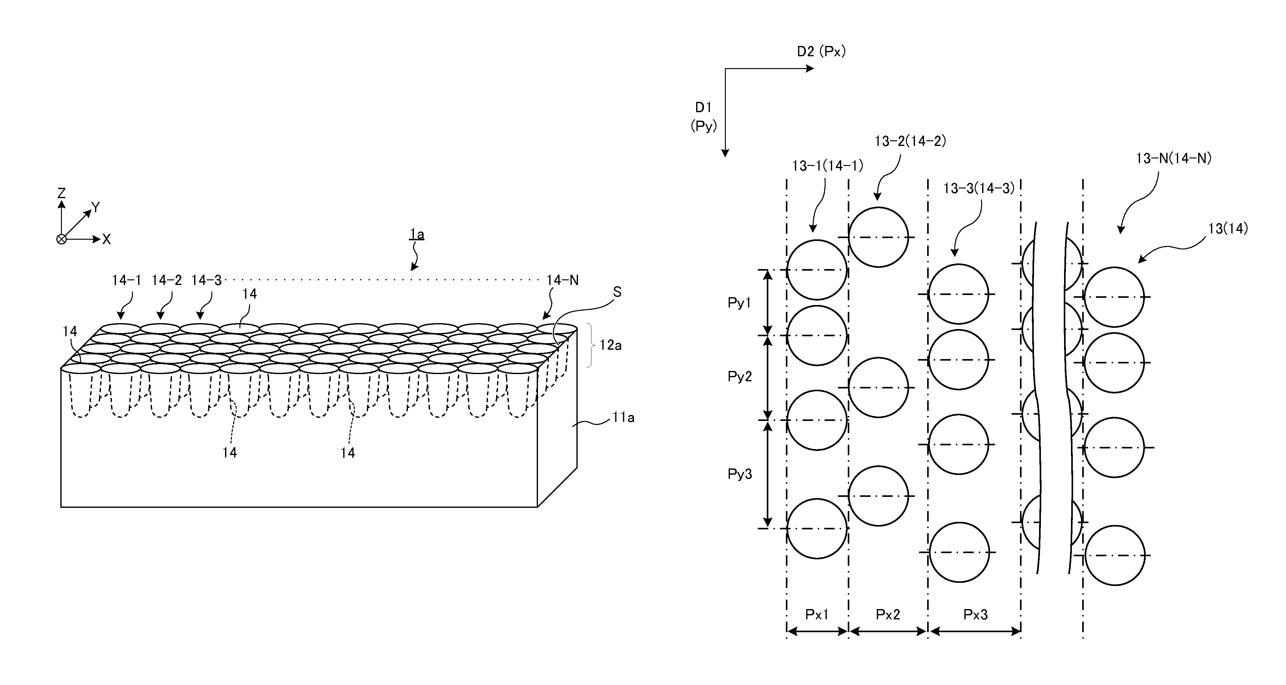
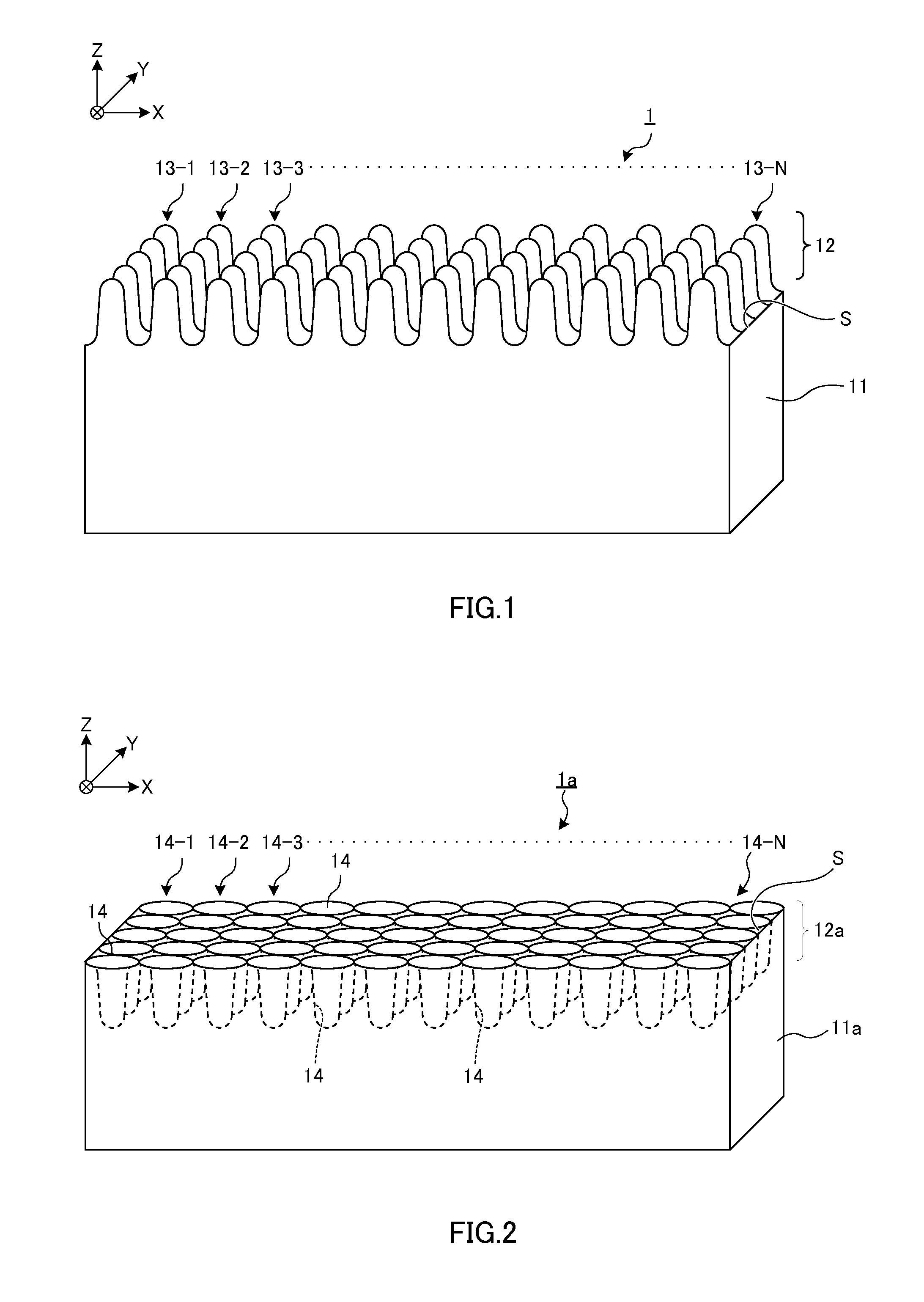
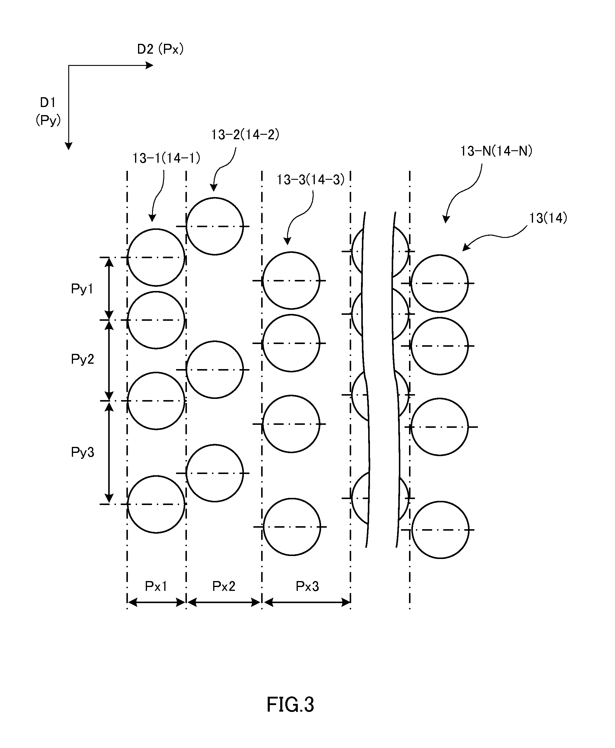

Image

  • Substrate for optics and light emitting device
  • Substrate for optics and light emitting device
  • Substrate for optics and light emitting device

Examples


example 1

Cylindrical Mold Preparation

Preparation of a Mold for Resin Mold Preparation

[0392]Used as a substrate of a cylindrical mold was a cylindrical quartz glass roll with a diameter of 80 mm and a length of 50 mm. A fine structure (fine concavo-convex structure) was formed on the cylindrical quartz glass roll surface by a direct-write lithography method using a semiconductor laser by the following method.

[0393]First, a resist layer is deposited on the fine structure on the quartz glass surface by a sputtering method. The sputtering method was carried out with power of RF 100 W using CuO (containing 8 atm % of Si) as a target (resist layer). The film thickness of the resist layer after deposition was 20 nm. The cylindrical mold prepared as described above was exposed on the following conditions while rotating at linear speed s=1.0 msec.

[0394]Exposure semiconductor laser wavelength: 405 nm

[0395]Exposure laser power: 3.5 mV

[0396]D2 direction pitch Px: 398 nm[0397]Variable width δ2 with respe...

example 2

[0428]A cylindrical mold prepared as in Example 1 was exposed on the following conditions while rotating at linear speed s=1.0 m / sec.

[0429]Exposure semiconductor laser wavelength: 405 nm

[0430]Exposure laser power: 3.5 mV

[0431]D2 direction pitch Px: 606 nm[0432]Variable width δ2 with respect to the D2 direction pitch Px: 61 nm[0433]Long period PxL in the D2 direction of the variable width δ2: 6 μm

[0434]D1 direction pitch Py: 700 nm[0435]Variable width δ1 with respect to the D1 direction pitch Py: 70 nm[0436]Long period PyL in the D1 direction of the variable width δ1: 7 μm

[0437]Next, as in Example 1, obtained was a reel-shaped transparent resin mold (length 200 m, width 300 mm) with the fine structure inversely transferred. Using the reel-shaped transparent resin mold, an organic EL device (Example 2) was prepared as in Example 1.

example 3

[0438]A cylindrical mold prepared as in Example 1 was exposed on the following conditions while rotating at linear speed s=1.0 m / sec.

[0439]Exposure semiconductor laser wavelength: 405 nm

[0440]Exposure laser power: 3.5 mV

[0441]D2 direction pitch Px: 700 nm

[0442]D1 direction pitch Py: 700 nm

[0443]Control of the reference signal of the pitch Py was made only initially.

[0444]Next, as in Example 1, obtained was a reel-shaped transparent resin mold (length 200 m, width 300 mm) with the surface structure inversely transferred.

[0445]The surface of the prepared reel-shaped transparent resin mold was observed with the scanning electron microscope. Convex portions were arranged in the shape of lines with the set pitch Py in the D1 direction. Further, the line-shaped convex portions were repeatedly provided with the predetermined pitch Px in the D2 direction. Furthermore, the shift amounts σ were irregular among line-shaped convex portions arranged adjacent to one another in the D2 direction.

[0...


PUM


Abstract

To provide a substrate for optics for enabling the color shift caused by diffraction of light to be reduced, a substrate for optics (12) is provided with a fine-structure layer including dots (31) comprised of a plurality of convex portions or concave portions extending in the direction of from a main surface of a substrate to outside the surface, the fine-structure layer has a plurality of dot lines in which a plurality of dots is arranged with a pitch (Py) in the first direction inside the main surface of the substrate, while having a plurality of dot lines in which a plurality of dots is arranged with a pitch (Px) in the second direction orthogonal to the first direction inside the main surface of the substrate, and both of the pitch Py and the pitch Px are inconstant intervals and are of nano-order.

Description

TECHNICAL FIELD[0001]The present invention relates to a substrate for optics applicable to organic EL used in a display, illumination and the like, and a light emitting device using the substrate.BACKGROUND ART[0002]In recent years, to improve luminous efficiency in a light emitting device such as organic EL, fluorescence and LED, improvements have been studied in light emitting materials, low voltage, light extraction efficiency and the like.[0003]As a method of improving light extraction efficiency, it is studied to introduce a light scattering layer and low refractive index layer in a light emitting device, and the like (Patent Documents 1 and 2). Further, such a method is known that the travel direction of light in the waveguide mode is polarized to the direction of the light emitting device surface using diffraction of light to improve light extraction efficiency (Patent Document 3). Furthermore, such a technique is invented that metal periodical grid structure or fine-particle...

Claims


Application Information

Patent Timeline
Patent Type & Authority Patents(United States)
IPC IPC(8): G02B5/18H01L51/00H01L51/52H05B33/02
CPCG02B5/1861G02B5/1809H01L51/0096H01L51/5262H05B33/02Y02E10/549H10K77/10H10K50/852H10K50/854H10K50/85
Inventor YAMAGUCHI, FUJITOKOIKE, JUNINOUE, NAOKI
Owner ASAHI KASEI E-MATERIALS CORPORATION
Learn More