Memory array and coupled TCAM architecture for improved access time during search operation
- Summary
- Abstract
- Description
- Claims
- Application Information
AI Technical Summary
Benefits of technology
Problems solved by technology
Method used
Image

Examples
example embodiments
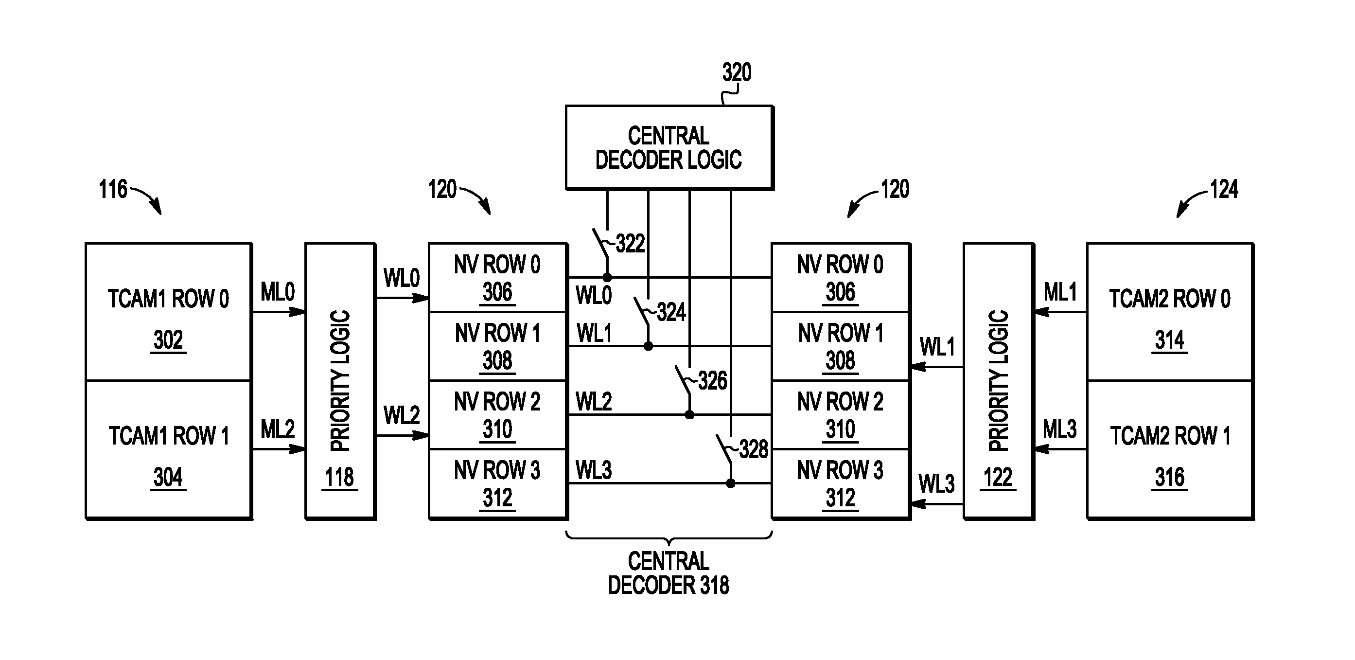
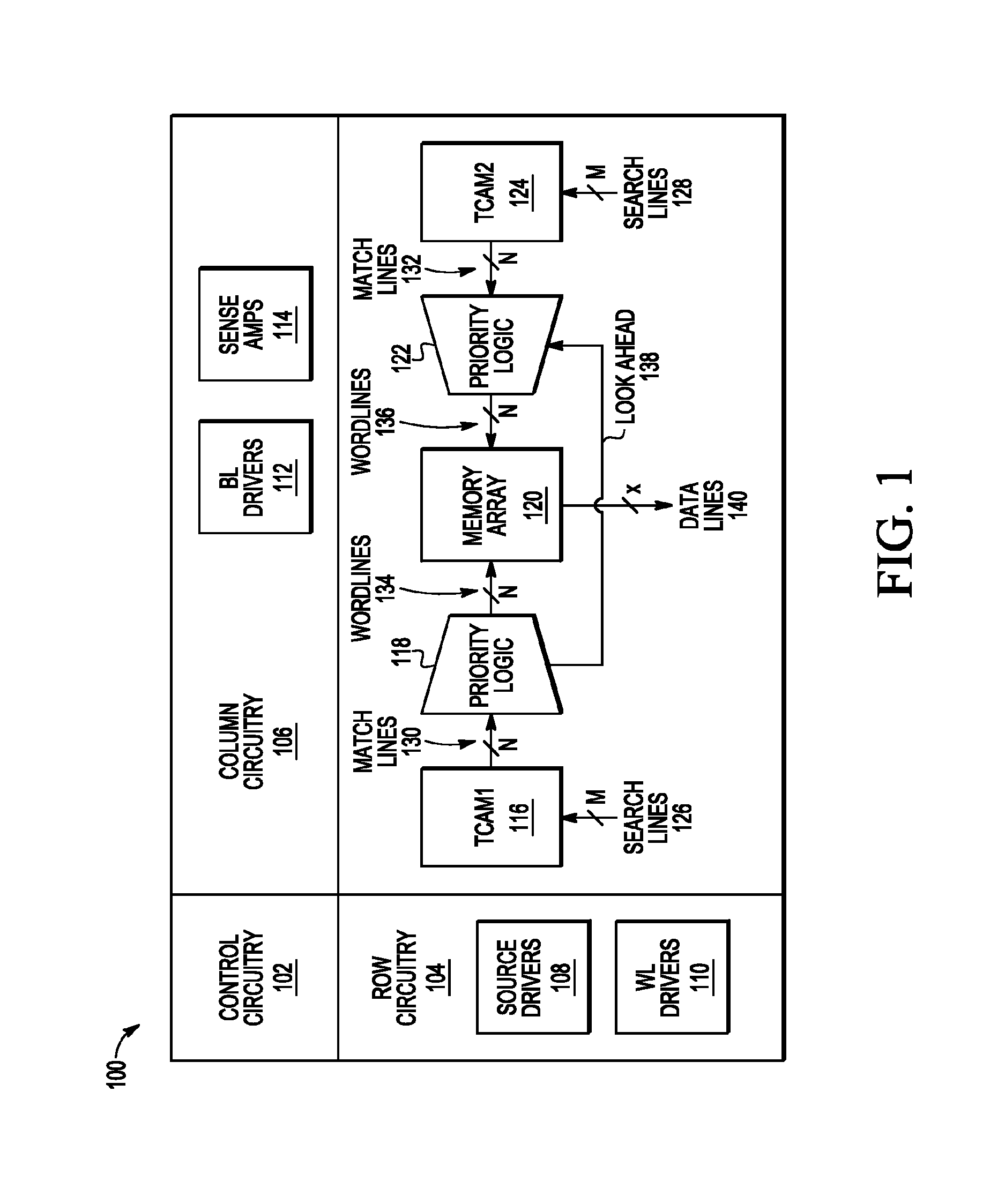
[0017]FIG. 1 illustrates a block diagram depicting an example memory device 100 in which the disclosure is implemented. In some embodiments, memory device 100 is implemented on a die or semiconductor substrate as part of a processing system. Memory device 100 includes control circuitry 102, row circuitry 104, column circuitry 106, a memory array 120, a first ternary content addressable memory (TCAM1) 116, a second ternary content addressable memory (TCAM2) 124, first priority logic 118, and second priority logic 122.
[0018]Control circuitry 102 is coupled to row circuitry 104 and to column circuitry 106. Row circuitry 104 and column circuitry 106 are each coupled to memory array 120, to TCAM1116, and to TCAM2124. Control circuitry 102 is also coupled to priority logic 118 and 122, and to a central decoder of memory array 120, as further discussed below. Control circuitry 102 is configured to control column circuitry 106 and row circuitry 104 to implement memory operations (e.g., read...
PUM
 Abstract
Description
Claims
Application Information
 - R&D
- Intellectual Property
- Life Sciences
- Materials
- Tech Scout
- Unparalleled Data Quality
- Higher Quality Content
- 60% Fewer Hallucinations
Browse by: Latest US Patents, China's latest patents, Technical Efficacy Thesaurus, Application Domain, Technology Topic, Popular Technical Reports.
© 2025 PatSnap. All rights reserved.Legal|Privacy policy|Modern Slavery Act Transparency Statement|Sitemap|About US| Contact US: help@patsnap.com