Wafer level packages with mechanically decoupled fan-in and fan-out areas

a technology of mechanical decoupling and wafer-level packages, applied in the direction of electrical equipment, semiconductor devices, semiconductor/solid-state device details, etc., can solve the problems of many wafer-level packages presenting reliability problems

Active Publication Date: 2017-01-10
INVENSAS CORP
View PDF24 Cites 3 Cited by
  • Summary
  • Abstract
  • Description
  • Claims
  • Application Information

AI Technical Summary

Benefits of technology

[0027]In one or more embodiments, the forming electrically conductive terminals and electrically conductive contacts can comprise depositing at least one dielectric layer overlying the surface of the molded region, and depositing an electrically conductive material onto the at least one dielectric layer.
[0028]In one or more embodiments, the terminals are first terminals, and the method may further comprise forming second termin

Problems solved by technology

Many wafer-level packages present reliability issues in such relatively larger sizes due to an inherent

Method used


Image

  • Wafer level packages with mechanically decoupled fan-in and fan-out areas
  • Wafer level packages with mechanically decoupled fan-in and fan-out areas
  • Wafer level packages with mechanically decoupled fan-in and fan-out areas

Examples


Embodiment Construction

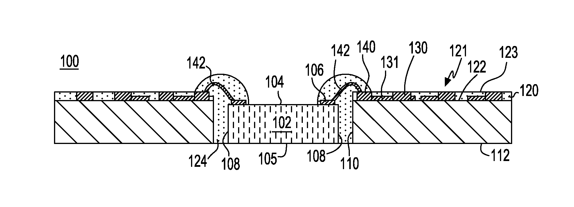
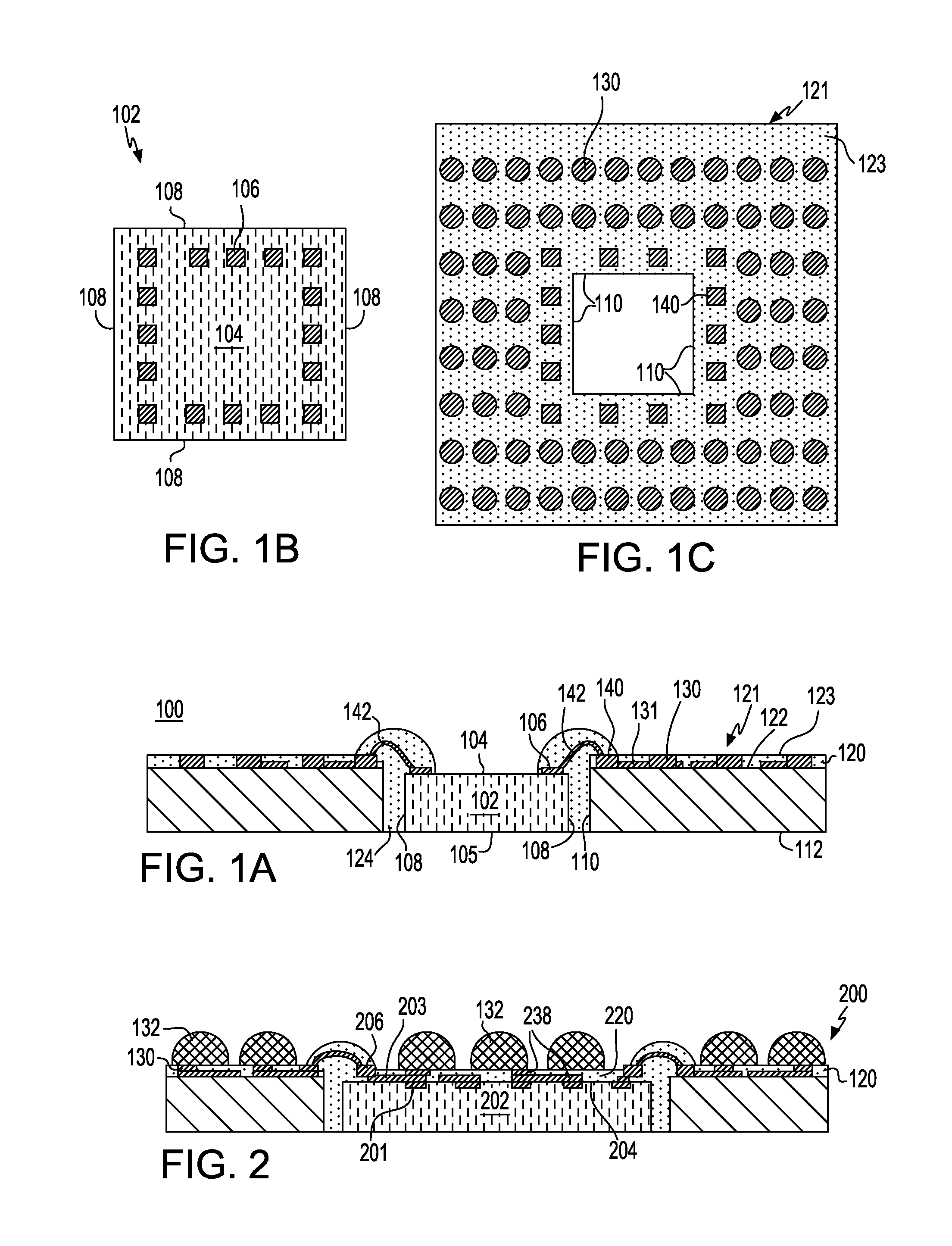
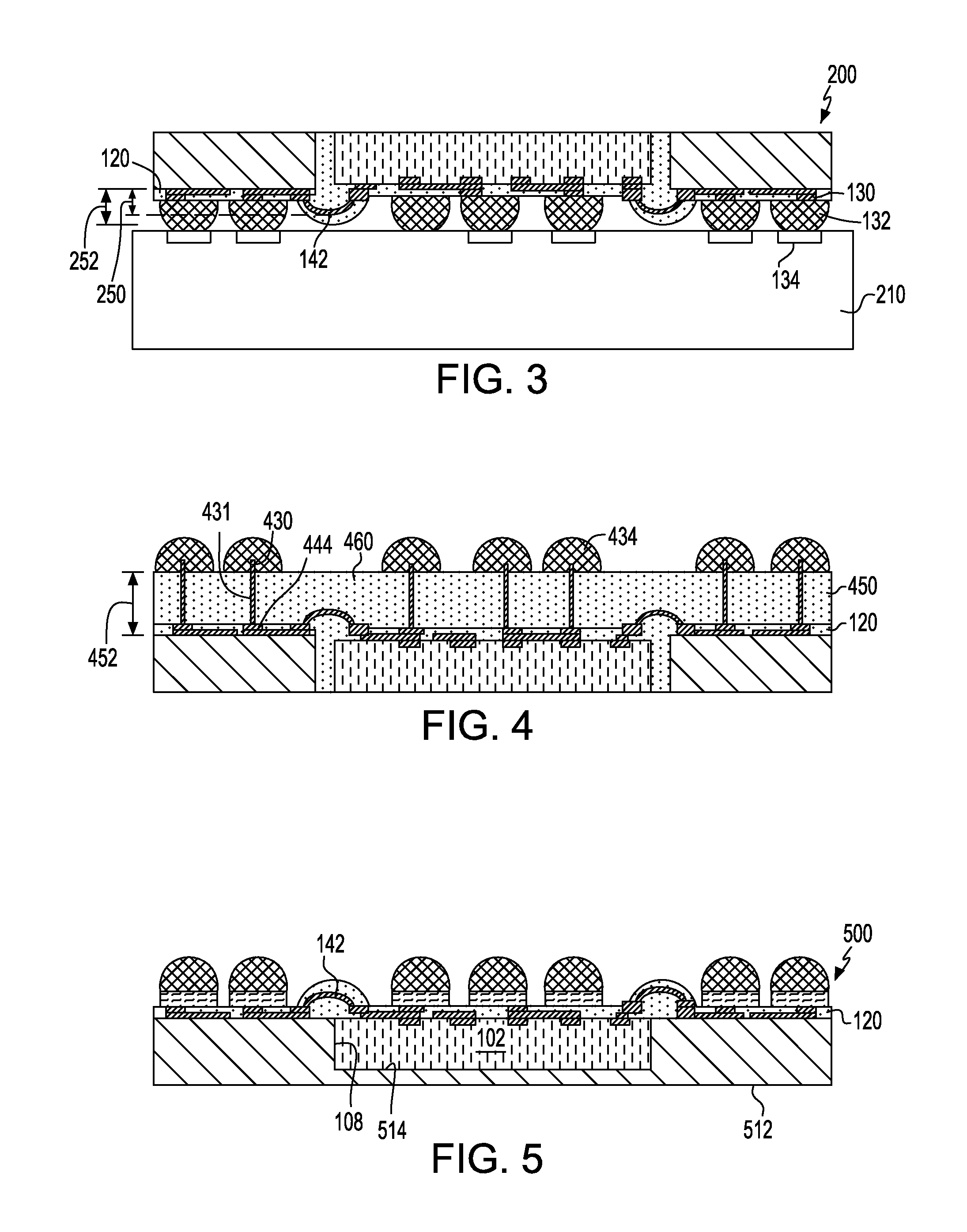
[0049]Referring to FIGS. 1A-1C, a fan-out microelectronic package 100 is provided in accordance with an embodiment of the invention. As seen in FIG. 1A, the package 100 includes a microelectronic element 102 having a front face 104, a plurality of bond pads 106 at the front face 104, and a rear face 105 opposite the front face. In an example as seen in FIG. 1A, the microelectronic element 102 is a bare semiconductor chip wherein a surface of the bare semiconductor chip is the face 104 of the microelectronic element, and the bond pads 106 are disposed at a surface of the semiconductor chip. As used in this disclosure with reference to a component, e.g., an interposer, microelectronic element, circuit panel, substrate, etc., a statement that an electrically conductive element is “at” a surface or face of a component indicates that, when the component is not assembled with any other element, the electrically conductive element is available for contact with a theoretical point moving in...


PUM


Abstract

A fan-out microelectronic package is provided in which bond wires electrically couple bond pads on a microelectronic element, e.g., a semiconductor chip which may have additional traces thereon, with contacts at a fan-out area of a dielectric element adjacent an edge surface of the chip. The bond wires mechanically decouple the microelectronic element from the fan-out area, which can make the electrical interconnections less prone to reliability issues due to effects of differential thermal expansion, such as caused by temperature excursions during initial package fabrication, bonding operations or thermal cycling. In addition, mechanical decoupling provided by the bond wires may also remedy other mechanical issues such as shock and possible delamination of package elements.

Description

BACKGROUND OF THE INVENTION[0001]Field of the Invention[0002]This application relates to fan-out microelectronic packages such as commonly known as fan-out wafer-level packages and methods of fabrication therefor.[0003]Description of the Related Art[0004]Semiconductor chips are commonly provided as individual, prepackaged units. A standard chip has a flat, rectangular body with a large front face having contacts connected to the internal circuitry of the chip. Each individual chip typically is mounted in a package which, in turn, is mounted on a circuit panel such as a printed circuit board and which connects the contacts of the chip to conductors of the circuit panel. In many conventional designs, the chip package occupies an area of the circuit panel considerably larger than the area of the chip itself. As used in this disclosure with reference to a flat chip having a front face, the “area of the chip” should be understood as referring to the area of the front face. In some design...

Claims


Application Information

Patent Timeline
IPC IPC(8): H01L25/065H01L23/00H01L23/31H01L25/00
CPCH01L25/0657H01L24/46H01L24/06H01L25/50H01L23/3128H01L24/43H01L24/03H01L2224/49171H01L2224/48091H01L2224/49112H01L2224/49111H01L2224/04042H01L2224/45015H01L2224/45144H01L2224/45147H01L2224/8592H01L2924/00014H01L2924/18165H01L21/568H01L2224/48157H01L2924/171H01L2224/48227H01L2924/15153H01L2224/85005H01L24/48H01L2224/48145H01L2224/49109H01L24/49H01L2224/96H01L2224/04105H01L24/20H01L2924/19107H01L23/13H01L23/49816H01L2924/20751H01L2924/2075H01L2924/20752H01L2924/20753H01L2924/20754H01L2924/20755H01L2924/20756H01L2924/20757H01L2924/20758H01L2924/20759H01L2924/2076H01L2224/05599
Inventor LEE, BONGSUBVU, TU TAMKATKAR, RAJESHMIRKARIMI, LAURA WILLSAGRAWAL, AKASHBANG, KYONG-MOGUEVARA, GABRIEL Z.LI, XUANHUYNH, LONG
Owner INVENSAS CORP
Why Eureka
Try Eureka