Oxide semiconductor film and method for forming oxide semiconductor film

a technology of oxide semiconductor and semiconductor film, which is applied in the direction of semiconductor devices, electrical devices, transistors, etc., can solve the problems of incomplete depletion of channel region, inability to crystallize region near the interface with the base, so as to achieve the effect of improving the crystallinity of oxide semiconductor

Active Publication Date: 2017-02-21
SEMICON ENERGY LAB CO LTD
View PDF134 Cites 1 Cited by
  • Summary
  • Abstract
  • Description
  • Claims
  • Application Information

AI Technical Summary

Benefits of technology

[0010]It is needless to say that the oxide semiconductor film can be made thick so that a crystalline region in a surface layer is used. In order to reduce parasitic capacitance and operate the transistor at low power consumption, however, the oxide semiconductor film needs to be made thin so that the channel region is completely depleted. In that case, conventional techniques, which have difficulty in crystallizing the immediate vicinity of the interface with the base, prevent miniaturization of transistors.
[0012]In order to solve the above problem, an object of one embodiment of the present invention is to improve crystallinity of an oxide semiconductor. Specifically, an object is to provide a crystalline oxide semiconductor film in which a crystallized region extends to the interface with a base or the vicinity of the interface and to provide a method for forming the crystalline oxide semiconductor film.
[0018]According to one embodiment of the present invention, crystallinity of an oxide semiconductor can be improved. In other words, a crystalline oxide semiconductor film in which a crystallized region extends to an interface with a base or the vicinity thereof, and a method for forming the oxide semiconductor film can be provided.

Problems solved by technology

In crystallization of oxide semiconductors and other semiconductors, there is a problem in that an amorphous region remains in the vicinity of the interface between a base and the semiconductor film to be crystallized.
In crystallization of an oxide semiconductor film formed on such an insulating material different from the oxide semiconductor, the problem arises in that a region near the interface with the base cannot be crystallized and an amorphous region remains.
In order to reduce parasitic capacitance and operate the transistor at low power consumption, however, the oxide semiconductor film needs to be made thin so that the channel region is completely depleted.
In that case, conventional techniques, which have difficulty in crystallizing the immediate vicinity of the interface with the base, prevent miniaturization of transistors.
Thus, even when the upper layer side of the oxide semiconductor film is crystallized, an amorphous region remains at the interface with the base insulating film, which has adversely affected the characteristics of transistors and the like.

Method used


Image

  • Oxide semiconductor film and method for forming oxide semiconductor film
  • Oxide semiconductor film and method for forming oxide semiconductor film
  • Oxide semiconductor film and method for forming oxide semiconductor film

Examples


example 1

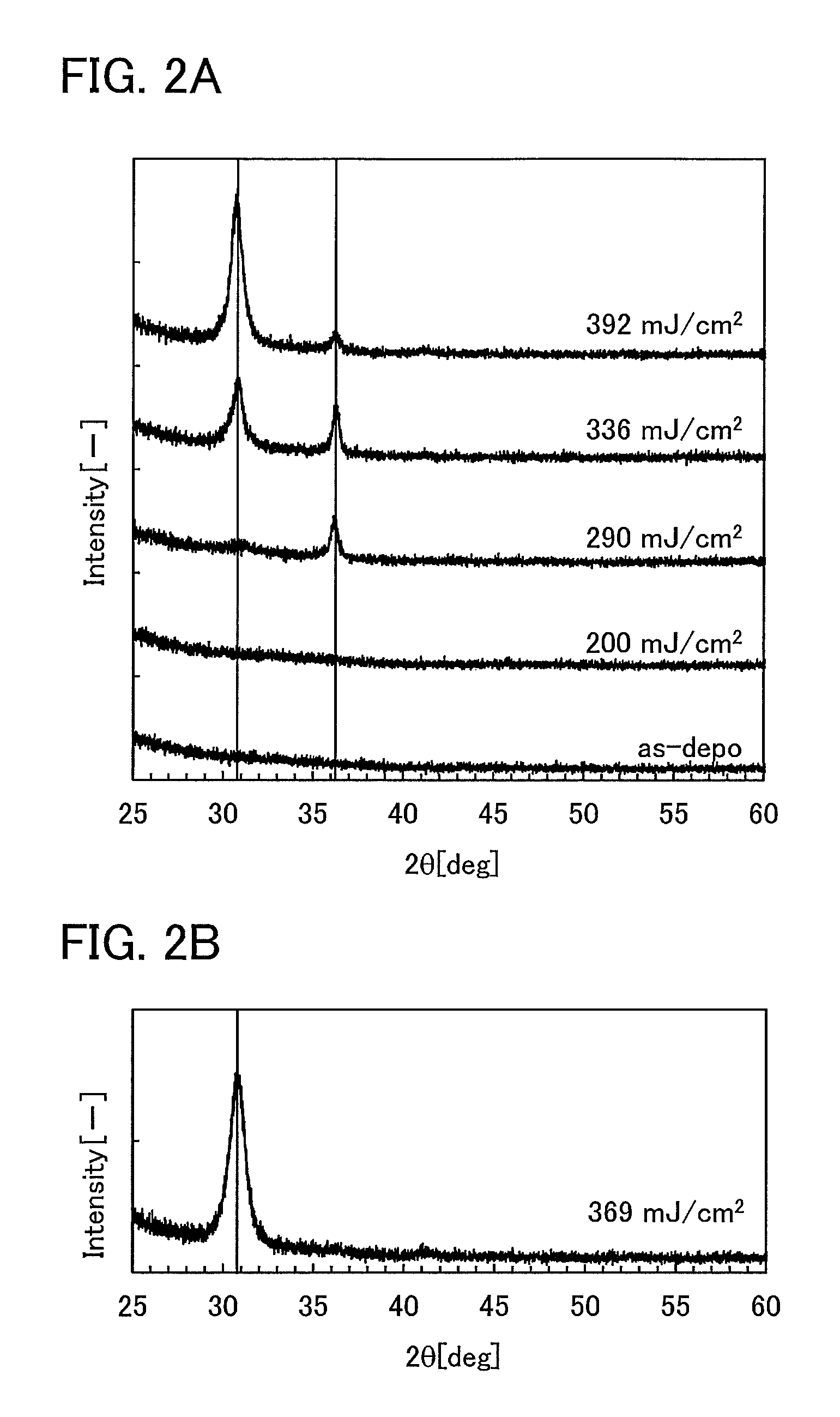
[0110]In Example 1, the attribution of a peak appearing at which 2θ was around 36° in crystallinity evaluation by an out-of-plane method using XRD was examined in detail.

[0111]Supposed planes to which a peak appearing at around 36° (2θ) is attributed are a (311) plane (2θ=35.7°) and a (222) plane (2θ=37.3°) in the case of an XRD pattern of ZnGa2O4 crystal with a spinel structure.

[0112]In order to cause a shift to a high-angle side in the (311) plane (2θ=35.7°), the lattice spacing needs to be narrowed. It is necessary for narrowing the lattice spacing to apply a high pressure. Thus, it is unlikely that the (311) plane is a plane having a peak at which 2θ is around 36°. On the other hand, when a Ga site in the ZnGa2O4 crystal is replaced with In, the lattice spacing on the (222) plane (2θ=37.3°) is expanded by In, and a shift to a low-angle side is caused. Thus, it is highly likely that the (222) plane is a plane having a peak at which 2θ is around 36°.

[0113]Cation radii of In hexaco...

example 2

[0125]In Example 2, atomic arrangement in cross sections of a surface layer and an inside of a nc-OS film irradiated with a laser beam was observed with a high-angle annular dark field scanning transmission electron microscopy (HAADF-STEM) and evaluated. A Hitachi scanning transmission electron microscope HD-2700 was used for the HAADF-STEM.

[0126]FIGS. 7A to 7C show atomic arrangement in a cross section of the surface layer of the nc-OS film. Note that FIG. 7A is a HAADF-STEM image, FIG. 7B is an enlarged view of a surrounded portion in FIG. 7A, and FIG. 7C shows a crystal structure model of InGaZnO4.

[0127]FIGS. 8A to 8C show atomic arrangement in a cross section of the inside of the nc-OS film. Note that FIG. 8A is a HAADF-STEM image, FIG. 8B is an enlarged view of a surrounded portion in FIG. 8A, and FIG. 8C shows a crystal structure model of ZnGa2O4.

[0128]According to FIGS. 7A to 7C, the cross section of the surface layer has the crystal structure of InGaZnO4. According to FIGS. ...

example 3

[0129]In Example 3, composition analysis of a CAAC-OS film and a nc-OS film that were In—Ga—Zn oxides were performed. Samples formed in this example are described.

[0130]First, a substrate was prepared. As a substrate of each sample, a quartz substrate was used. Then, an oxide semiconductor film (CAAC-OS film or nc-OS film) was formed over the substrate. The oxide semiconductor film was formed under the following conditions: a metal oxide target having an atomic ratio of In:Ga:Zn=1:1:1 (atomic ratio) was used as a sputtering target; argon and oxygen were supplied to a treatment chamber of a sputtering apparatus as a sputtering gas at flow rates of 30 sccm and 15 sccm, respectively; the pressure in the treatment chamber was controlled to 0.4 Pa; and a DC power of 0.5 kW was supplied. In addition, for formation of the nc-OS film, the substrate temperature at which the In—Ga—Zn oxide film was deposited was set to room temperature (25° C.). Further, for formation of the CAAC-OS film, the...


PUM


Abstract

To improve crystallinity of an oxide semiconductor. To provide a crystalline oxide semiconductor film in which a crystallized region extends to the interface with a base or the vicinity of the interface, and to provide a method for forming the oxide semiconductor film. An oxide semiconductor film containing indium, gallium, and zinc is formed, and the oxide semiconductor film is irradiated with an energy beam, thereby being heated. Note that the oxide semiconductor film includes a c-axis aligned crystal region or microcrystal.

Description

BACKGROUND OF THE INVENTION[0001]1. Field of the Invention[0002]The present invention relates to an oxide semiconductor film and a method for forming an oxide semiconductor film.[0003]2. Description of the Related Art[0004]An oxide semiconductor has attracted attention as a material for transistors. The oxide semiconductor is said to have a feature similar to that of amorphous silicon capable of being formed at a low temperature, and a feature similar to that of polycrystalline silicon having high field-effect mobility. For example, the following is disclosed: a field-effect transistor using an amorphous oxide, whose electron carrier concentration is controlled, and an image display device using the transistor (Patent Document 1).[0005]The transistor using an amorphous oxide semiconductor formed at room temperature, however, has a problem in characteristics: not enough high field-effect mobility, low reliability, and large hysteresis. In order to solve such a problem, a technique of...

Claims


Application Information

Patent Timeline
Patent Type & Authority Patents(United States)
IPC IPC(8): H01L21/00H01L29/786H01L21/02H01L29/66
CPCH01L29/7869H01L21/02554H01L21/02565H01L21/02631H01L21/02678H01L21/02686H01L29/66969
Inventor SHIMOMURA, AKIHISAISHIYAMA, TAKAHISAKOYAMA, MASAKIKIKUCHI, ERUMUHIROHASHI, TAKUYAOOTA, MASASHI
Owner SEMICON ENERGY LAB CO LTD
Why Eureka
Try Eureka