Optical transmitter or transmission unit in optical transmitter/receiver provided on opto-electric hybrid board

a technology of optical transmitter and transmission unit, which is applied in the direction of optical elements, semiconductor lasers, instruments, etc., can solve the problems of emi (electromagnetic radiation noise), signal delay due to electric wiring, and generation of heat, so as to achieve more effective and free transmission, reduce the load on electric wiring for high-speed/high-frequency use, and suppress the deterioration of the above explained electrical wiring

Active Publication Date: 2017-02-21
AIO CORE CO LTD
View PDF9 Cites 0 Cited by
  • Summary
  • Abstract
  • Description
  • Claims
  • Application Information

AI Technical Summary

Benefits of technology

[0016]According to the basic construction of the present invention, in the optical transmitter or the transmission unit in the optical transmitter / receiver provided on the opto-electric hybrid board, the semiconductor laser is placed on an output side of the optical modulators, i.e., it is placed near the optical signal outputting parts, in the optical integrated circuit; so that electric wire connection of electrical signal wiring lines, that is highly dependent on frequencies, can be carried out more effectively and freely. Thus, load on the electric wiring for high-speed / high-frequency use can be reduced. Further, by having an optical pin as an optical interface, deterioration of the above explained electrical wiring can be suppressed, and low-loss coupling to an external waveguide such as a fiber or the like can be carried out without having effect due to placement of the semiconductor laser and / or the driver IC. By guiding the light from the semiconductor laser to the optical modulators by use of optical waveguides that are placed in spaces between optical modulators, and by making the connection length of each of the plural optical waveguides to be equal the optical waveguides to be isometric, the wiring length can be reduced, uniformity of optical losses can be realized, crosstalk in the receiver side can be suppressed, and optical interconnection having good signal quality can be realized, when compared with the case that wiring is carried out to avoid the driver IC and / or the whole of optical modulators.
[0017]As a result, the present invention can realize an optical transmitter or a transmission unit in an optical transmitter / receiver having good high-frequency characteristics.

Problems solved by technology

Recently, problems such as signal delay due to electric wiring, generation of heat, generation of EMI (electromagnetic radiation noise), and so on have been surfaced in the connection between electronic devices such as boards, computers, peripheral devices, and so on.

Method used


Image

  • Optical transmitter or transmission unit in optical transmitter/receiver provided on opto-electric hybrid board
  • Optical transmitter or transmission unit in optical transmitter/receiver provided on opto-electric hybrid board
  • Optical transmitter or transmission unit in optical transmitter/receiver provided on opto-electric hybrid board

Examples


Embodiment Construction

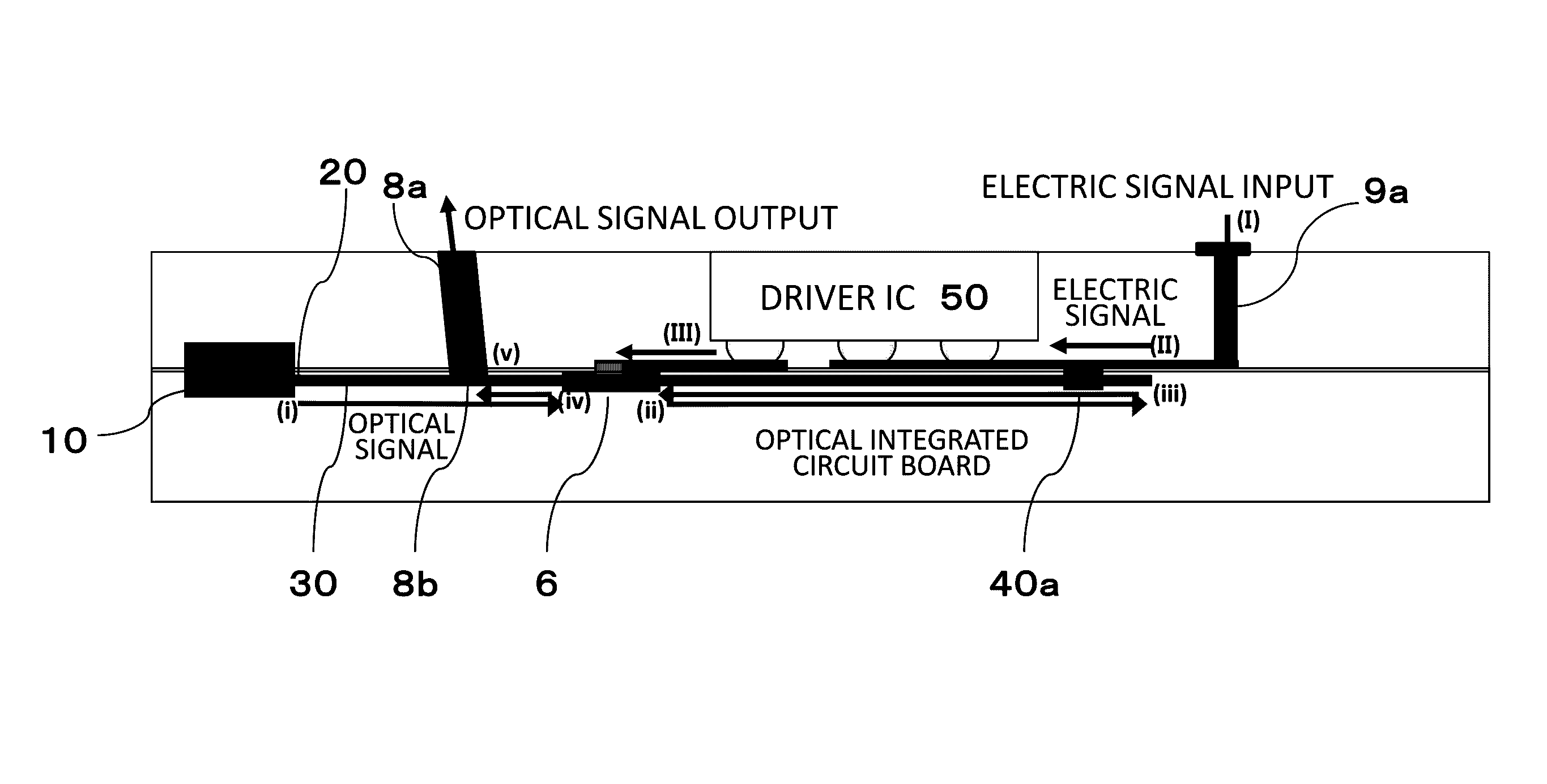
[0030]In the following, an optical transmitter or a transmission unit in an optical transmitter / receiver provided on an opto-electric hybrid board according to each of embodiments of the present invention will be explained in detail with reference to the figures. Note that, although an optical transmitter is considered mainly as the basis of explanation, the explanation also applies to a transmission unit in an optical transmitter / receiver. Also, similar reference symbols are assigned to similar components.

[0031]Each of FIGS. 3-5 is a schematic plain view showing an optical integrated circuit 200 for an optical transmitter provided on an opto-electric hybrid board, according to an embodiment of the present invention. FIG. 3 shows an aspect of arrangement of optical elements; and this figure corresponds to FIG. 1 that shows a prior-art construction. On the other hand, FIG. 4 does not show optical waveguide elements and so on; however, instead thereof, it shows arrangement of circuit ...


PUM

PropertyMeasurementUnit
bend angleaaaaaaaaaa
sizeaaaaaaaaaa
sizeaaaaaaaaaa

Abstract

This present invention is provided with: a semiconductor laser for emitting laser light in a plurality of channels; optical waveguides optically coupled in a corresponding manner to the semiconductor lasers, the optical waveguides propagating laser light as input light for each channel; optical modulators for modulating the input light and generating an optical signal; and an optical signal output unit coupled to the optical modulators, the optical signal output unit outputting the optical signal propagated from the optical modulators to the exterior. The present invention is characterized in that the semiconductor laser is arranged on the opposite side from an optical branching unit and the optical modulators, with the optical signal output unit interposed therebetween, in the plane of an opto-electric hybrid board.

Description

TECHNICAL FIELD[0001]The present invention relates to an optical transmitter or a transmission unit in an optical transmitter / receiver provided on an opto-electric hybrid board, and, more specifically, the present invention relates to an optical integrated circuit, that is characterized in placement of a semiconductor laser and arrangement of optical waveguides, in the optical transmitter or the transmission unit in the optical transmitter / receiver.BACKGROUND ART[0002]Recently, problems such as signal delay due to electric wiring, generation of heat, generation of EMI (electromagnetic radiation noise), and so on have been surfaced in the connection between electronic devices such as boards, computers, peripheral devices, and so on. For solving such problems arising in electric wiring, optical interconnection, that is constructed by use of a silicon photonics technique, is being developed (Non-patent-related Document 1). The silicon photonics is a technique relating to optical elemen...

Claims


Application Information

Patent Timeline
Patent Type & Authority Patents(United States)
IPC IPC(8): G02B6/28G02F1/025G02B6/42H01S5/022G02B6/125H01S5/026H01S5/00G02B6/12G02B6/34
CPCH01S5/0268G02B6/12004G02B6/125G02B6/4204G02B6/4249G02F1/025H01S5/0085H01S5/02248G02B2006/12142H01S5/005G02B6/2813G02B6/34H01S5/02325
Inventor YASHIKI, KENICHIROKURATA, KAZUHIKO
Owner AIO CORE CO LTD
Why Eureka
Try Eureka