Etch removal of current distribution layer for LED current confinement

a technology of led current confinement and current distribution layer, which is applied in the direction of semiconductor devices, semiconductor/solid-state device details, instruments, etc., can solve the problem of low efficiency

Active Publication Date: 2017-02-28
APPLE INC
View PDF178 Cites 41 Cited by
  • Summary
  • Abstract
  • Description
  • Claims
  • Application Information

AI Technical Summary

Problems solved by technology

At low current density the efficiency is low due to the strong effect of defects or other processes by which electrons and holes recombine without the generation of light, called non-radiative recombination.

Method used


Image

  • Etch removal of current distribution layer for LED current confinement
  • Etch removal of current distribution layer for LED current confinement
  • Etch removal of current distribution layer for LED current confinement

Examples


example 1

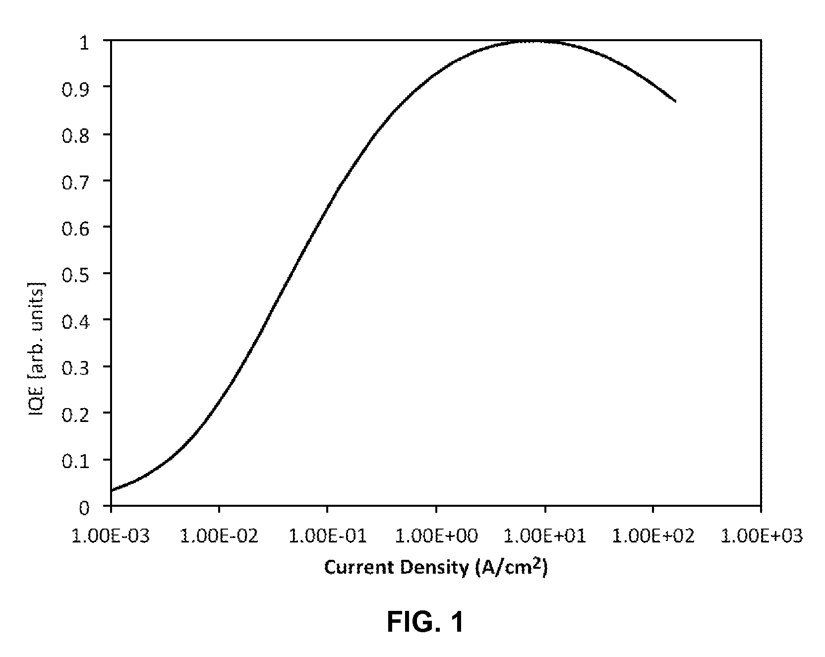
[0090]In one embodiment, a display panel is a 5.5 inch full high definition display with 1920×1800 resolution, and 400 pixels per inch (PPI) including a 63.5 μm RGB pixel size. To achieve a 300 Nit output (white) with LED devices having a 10% EQE, the display panel uses approximately 10 nA-30 nA of current per LED, assuming one LED per subpixel. For an LED device with a 10 μm×10 μm confined current injection area this corresponds to a current density of 0.01 A / cm2-0.03 A / cm2. This is well below the normal or designed operating conditions for standard LEDs.

example 2

[0091]In an embodiment, the parameters of Example 1 are the same, with a smaller 1 μm×1 μm confined current injection area. With this reduced current injection area the corresponding current density increases to 1 A / cm2-3 A / cm2. Thus, Example 2 illustrates that at operating currents of 10 nA-30 nA, small changes in current injection area from 10 μm×10 μm to 1 μm×1 μm can have a significant effect on current density. In turn, the change in current density may affect efficiency of the LED device.

example 3

[0092]In one embodiment, a display panel is a 5.5 inch full high definition display with 1920×1800 resolution, and 400 pixels per inch (PPI) including a 63.5 μm RGB pixel size. Each subpixel includes an LED device with a 10 μm×10 μm confined current injection area. Luminance is maintained at 300 Nit output (white). In this example, it is desired to achieve a 40% EQE. With this increased efficiency, lower operating currents may be used. In an embodiment, an operating current of 3 nA-6 nA per LED is selected. With these parameters an LED device with a 10 μm×10 μm confined current injection area operates at 0.003 A / cm2-0.006 A / cm2, and an LED device with a 1 μm×1 μm confined current injection area operates at 0.3 A / cm2-0.6 A / cm2.


PUM


Abstract

A method and structure for forming an array of LED devices is disclosed. The LED devices in accordance with embodiments of the invention may include a confined current injection area in which a current spreading layer protrudes away from a cladding layer in a pillar configuration so that the cladding layer is wider than the current spreading layer pillar.

Description

BACKGROUND[0001]Field[0002]The present invention relates to light emitting diode (LED) devices. More particularly, embodiments of the invention relate to LED devices with a confined current injection area.[0003]Background Information[0004]Light emitting diodes (LEDs) are increasingly being considered as a replacement technology for existing light sources. For example, LEDs are found in signage, traffic signals, automotive tail lights, mobile electronics displays, and televisions. Various benefits of LEDs compared to traditional lighting sources may include increased efficiency, longer lifespan, variable emission spectra, and the ability to be integrated with various form factors.[0005]One type of LED is an organic light emitting diode (OLED) in which the emissive layer of the diode is formed of an organic compound. One advantage of OLEDs is the ability to print the organic emissive layer on flexible substrates. OLEDs have been integrated into thin, flexible displays and are often us...

Claims


Application Information

Patent Timeline
Patent Type & Authority Patents(United States)
IPC IPC(8): H01L25/075H01L33/00H01L33/14G09G3/32H01L23/00H01L33/20
CPCH01L25/0753G09G3/32H01L24/75H01L24/95H01L33/0079H01L33/14H01L33/0095H01L33/20H01L2924/0002H01L2924/12041H01L2924/12042H01L2924/12044H01L2924/00H01L33/0093
Inventor MCGRODDY, KELLYHU, HSIN-HUABIBL, ANDREASCHAN, CLAYTON KA TSUN
Owner APPLE INC
Why Eureka
Try Eureka