Apparatus and method for highly controlled electrodeposition

a technology of electroplating substrates and apparatuses, which is applied in the direction of evaporation applications, soldering apparatuses, manufacturing tools, etc., can solve the problems of inferior to a metallic ion source, insufficient control of the deposition process, and easy variation of operating geometries and other parameters of the cell

Inactive Publication Date: 2004-12-23
COOK BIOTECH +1
View PDF40 Cites 39 Cited by
  • Summary
  • Abstract
  • Description
  • Claims
  • Application Information

AI Technical Summary

Problems solved by technology

Configurations of this type do not provide sufficient control over the deposition process to enable the uniform plating of submicron features on a substrate.
Nor can the operating geometries and other parameters of the cell be easily varied to accommodate different types of plating substrates or patterns, or to adjust the plating conditions to ensure uniformity and quality of the deposit.
Another drawback of the existing art is that in order to place the anode close to the cathode, an insoluble anode must be used with a metal salt solution, which is inferior to a metallic ion source.
Alternatively, a soluble metallic anode may be used, but it cannot be placed close to the cathode because of potential contamination.
In addition, as the anode dissolves it changes shape, reducing the very control of the deposit parameters that was provided by choosing the initial shape of the anode.

Method used


Image

  • Apparatus and method for highly controlled electrodeposition
  • Apparatus and method for highly controlled electrodeposition
  • Apparatus and method for highly controlled electrodeposition

Examples


Embodiment Construction

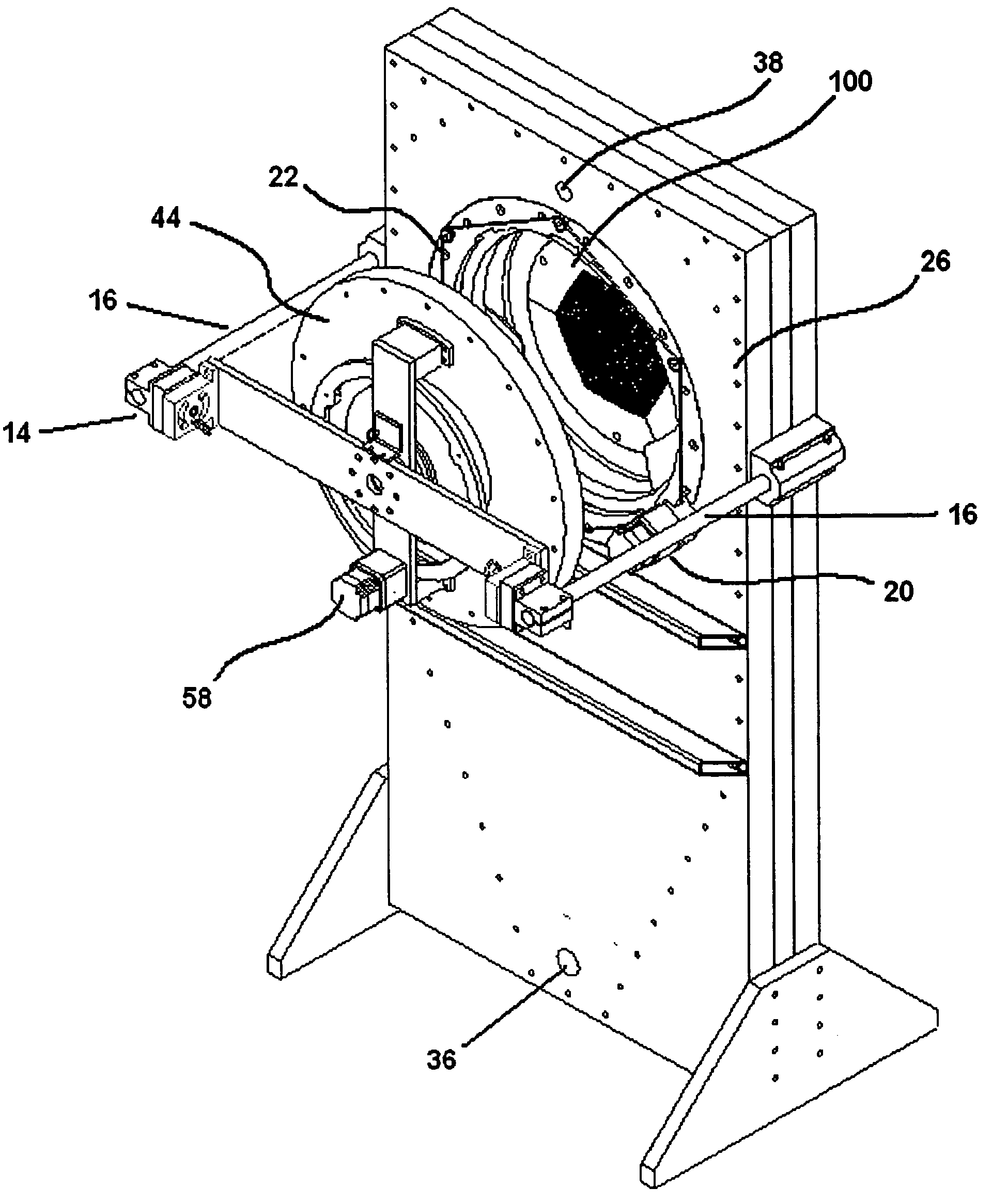
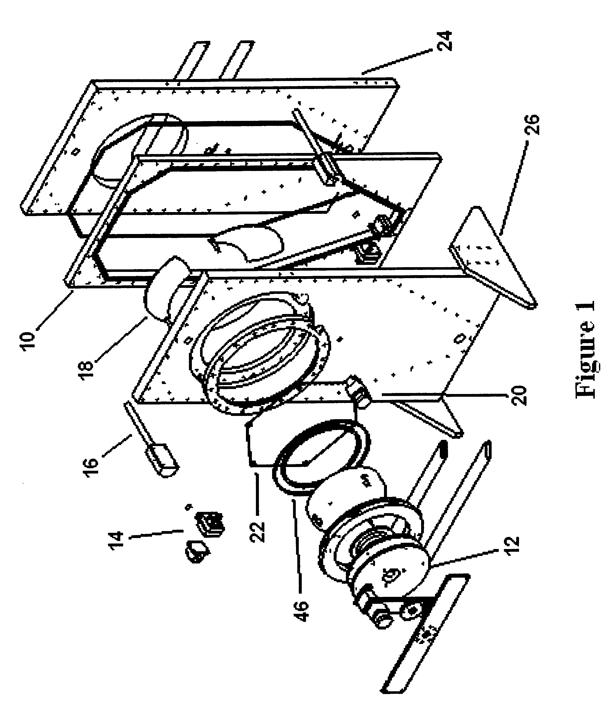
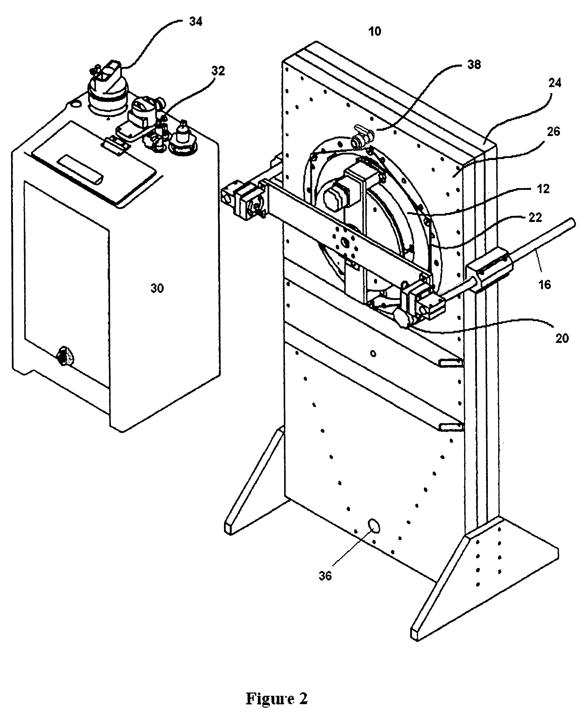
[0048] The present invention is of an apparatus and method for highly controlled electrodeposition, particularly useful for electroplating submicron structures. Enhanced control of the process provides for a more uniform deposit thickness over the entire substrate, and permits reliable plating of submicron features, for example those on a semiconductor wafer. A primary advantage of the invention is that the kinetics of the cell, which are based on the geometries of the cell, can be changed quickly to optimize plating on the substrate surface, for all deposits including very thick film deposits and thin film deposits.

[0049] As used throughout the specification and claims, "substrate" means any substrate, wafer, lens, panel, and the like, or any other item which is to be attached to an electrode to be plated. Such substrate may comprise any material such as a semiconductor, including but not limited to silicon, gallium arsenide, sapphire, glass, ceramic, metal alloy, polymer, or photo...


PUM

PropertyMeasurementUnit
pressureaaaaaaaaaa
pressureaaaaaaaaaa
diameteraaaaaaaaaa

Abstract

An apparatus and method for highly controlled electrodeposition, particularly useful for electroplating submicron structures. Enhanced control of the process provides for a more uniform deposit thickness over the entire substrate, and permits reliable plating of submicron features. The apparatus includes a pressurized electrochemical cell to improve plating efficiency and reduce defects, vertical laminar flow of the electrolyte solution to remove surface gases from the vertically arranged substrate, a rotating wafer chuck to eliminate edge plating effects, and a variable aperture to control the current distribution and ensure deposit uniformity across the entire substrate. Also a dynamic profile anode whose shape can be varied to optimize the current distribution to the substrate. The anode is advantageously able to use metallic ion sources and may be placed close to the cathode thus minimizing contamination of the substrate.

Description

[0001] This application claims the benefit of the filing of U.S. Provisional Patent Application Ser. No. 60 / 431,315, entitled "Solid Core Solder Particles for Printable Solder Paste", filed on Dec. 5, 2002, U.S. Provisional Patent Application Ser. No. 60 / 447,175, entitled "Electrochemical Devices and Processes", filed on Feb. 12, 2003, and U.S. Provisional Patent Application Ser. No. 60 / 519,813, entitled "Particle Coelectrodeposition", filed on Nov. 12, 2003. This application also is a continuation-in-part of U.S. patent application Ser. No. 10 / 728,636, entitled "Coated and Magnetic Particles and Applications Thereof", filed Dec. 5, 2003. The specifications of each application listed are incorporated herein by reference.[0002] 1. Field of the Invention (Technical Field)[0003] The present invention relates to an apparatus and method for electroplating substrates or other objects, particularly semiconductor wafers. The present invention can also be used to plate ceramic panels used in...

Claims


Application Information

Patent Timeline
Patent Type & Authority Applications(United States)
IPC IPC(8): B23K35/02C25D7/12C25D17/16H01F41/16H01F41/20H01F41/26H05K3/34
CPCB22F2998/00C25D17/001B23K35/0244C25D15/00C25D15/02H01F41/16H01F41/20H01F41/26H01L2924/01027B22F2999/00H01L2924/014H01L2924/01006H01L2924/01005H01L2224/11334B22F1/025B22F1/0088B22F1/17B22F1/145
Inventor GRIEGO, THOMAS P.SANCHEZ, FERNANDO M.
Owner COOK BIOTECH
Why Eureka
Try Eureka