

Method for forming silicon oxide cap layer for solid state diffusion process
a technology of silicon oxide and solid state diffusion, which is applied in the direction of basic electric elements, electrical apparatus, plasma techniques, etc., can solve the problems of insufficient diffusion of dopants in the substrate, inability to achieve the desired level of dopants dispersion in the substrate in ssd, and insufficient thickness of the cap film, etc., to achieve the effect of inhibiting the dispersion of dopants, and improving the quality of the film
- Summary
- Abstract
- Description
- Claims
- Application Information
AI Technical Summary
Benefits of technology
Problems solved by technology
Method used
Image

Examples
reference example 1
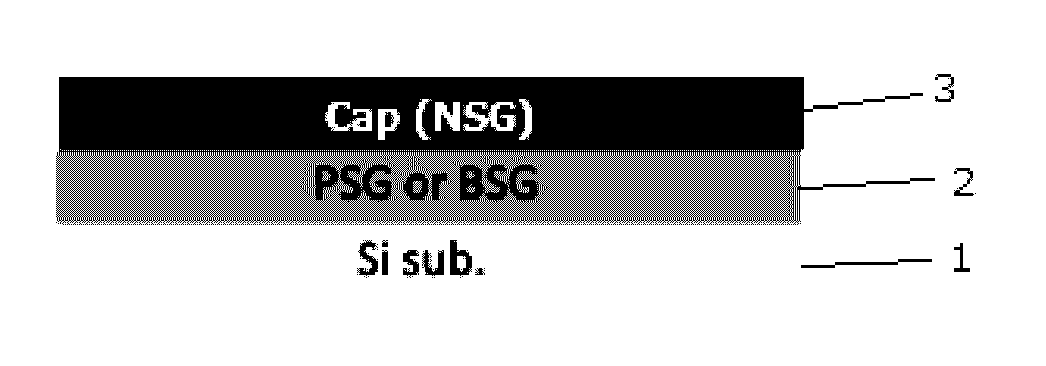
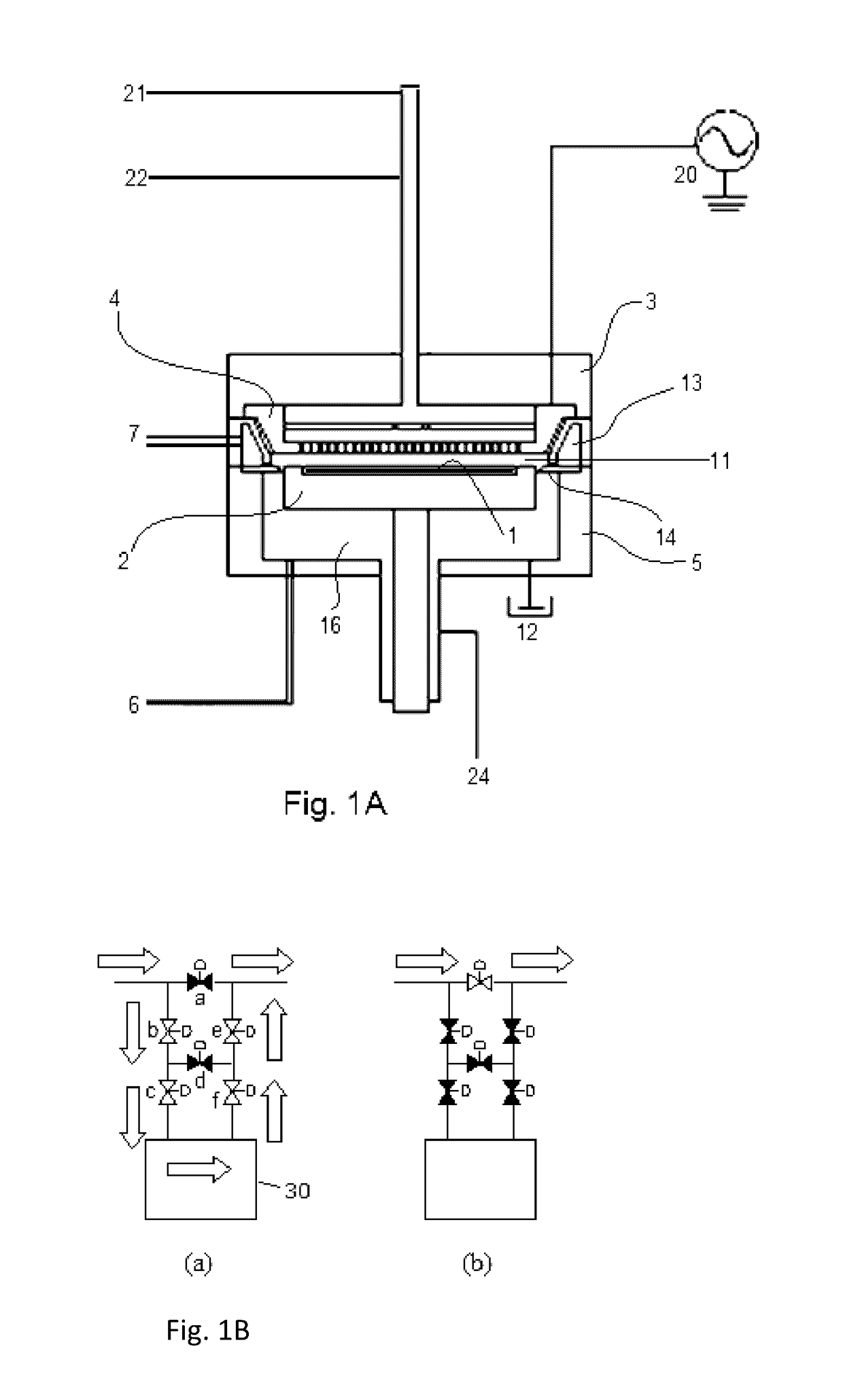
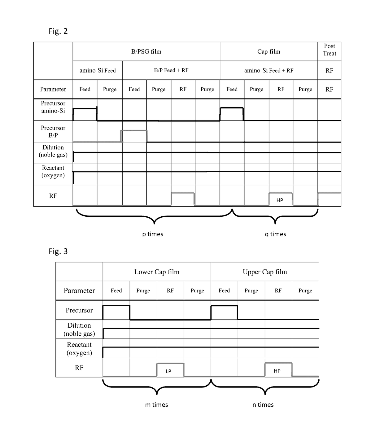
[0075]A SiO cap film was deposited on a BSG film having a thickness of 5 nm formed on a Si substrate (0300 mm) by PEALD using the PEALD apparatus illustrated in FIG. 1A (including a modification illustrated in FIG. 1B) under conditions shown in Table 6 below with the sequence illustrated in FIG. 2 except that no post-deposition plasma treatment was conducted and RF power was not high, i.e., the SiO cap film was considered to be a standard cap film.
[0076]
TABLE 6(numbers are approximate)BSG filmAminoSi B Feed + Cap FeedRFSiODepo rateSiO [times]10NAB [times]03Bottle Temp[° C.]35.035.050.0BTL Ar[sccn]2,0002,0002,000O2 / DCM[sccm]1,0001,0001,000Ar / DCM[sccm]1,0001,0001,000Seal He / DCM[sccm]200200200RC Press[Pa]400400400HRF[W]NA200200SUS Temp[° C.]300300300SHD Temp[° C.]150150150Wal Temp[° C.]130130130Gap[mm]7.57.57.5Shift time [sec]Source Feed0.30.30.2Source Purge0.40.40.3RF-ON00.20.2Post Purge00.10.1Cycle time [sec]0.71.00.8
[0077]In the table, “AminoSi Feed” denotes a step of forming a SiO ...
example 1
[0081]Each of SiO cap films (g, h, i, and j) was deposited on a BSG film having a thickness of 2 nm formed on a Si substrate (0300 mm) by PEALD using the PEALD apparatus illustrated in FIG. 1A (including a modification illustrated in FIG. 1B) under conditions shown in Table 7 below with the sequence illustrated in FIG. 2 or 3 as follows:
[0082]g) the sequence of FIG. 2 except that no post-deposition plasma treatment was conducted, wherein the thickness of the cap film was 2 nm;
[0083]h) the sequence of FIG. 2 wherein post-deposition plasma treatment 1 was conducted, and the thickness of the cap film was 2 nm;
[0084]i) the sequence of FIG. 2 wherein post-deposition plasma treatment 2 was conducted, and the thickness of the cap film was 2 nm; and
[0085]j) the sequence of FIG. 2 modified by FIG. 3 except that no post-deposition plasma treatment was conducted, wherein the thickness of the lower cap film was 1 nm and the thickness of the upper cap film was 1 nm.
[0086]After the completion of ...
example 2
[0090]In this example, three cap films were deposited each on a BSG film formed on a Si substrate (Φ300 mm) by PEALD, in a manner substantially similar to that shown in Table 7:
[0091]k) the thickness of BSG film was 2 nm, and the sequence illustrated in FIG. 2 was conducted;
[0092]m) the thickness of BSG film was 1 nm, and the sequence illustrated in FIG. 2 was conducted; and
[0093]n) the thickness of BSG film was 1 nm, and the sequence illustrated in FIG. 2 modified by the sequence illustrated in FIG. 3 was conducted.
[0094]The thickness of each substrate was measured as layering took place. The results are shown in Tables 8 (k), 9 (m), and 10 (n) below.
[0095]
TABLE 8(numbers are approximate)Target Measured k) Layer structuresthicknessthickness [nm]Native oxide1.24Si waferBSG2 nm3.40Native oxideSi waferHigh-quality Cap2 nm5.60BSG2 nmNative oxideSi waferPost-deposition—5.67plasma treatmentHigh-quality Cap2 nmBSG2 nmNative oxideSi wafer
[0096]
TABLE 9(the numbers are approximate)Target Mea...
PUM
 Abstract
Description
Claims
Application Information