Semiconductor light emitting device

a technology of light emitting device and semiconductor, which is applied in the direction of semiconductor devices, basic electric elements, electrical equipment, etc., can solve the problems of insufficient improvement of light extraction efficiency and restricted effect, and achieve excellent light extraction efficiency, light extraction efficiency can be remarkably enhanced, and back scattering light can be reduced

Inactive Publication Date: 2017-03-28
SCHOTT AG
View PDF44 Cites 2 Cited by
  • Summary
  • Abstract
  • Description
  • Claims
  • Application Information

AI Technical Summary

Benefits of technology

[0018]The present invention is conducted in consideration of such circumstance and an object thereof is to provide a semiconductor light emitting device excellent in light extraction efficiency.
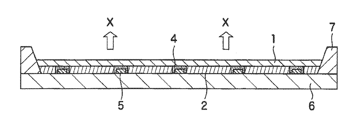
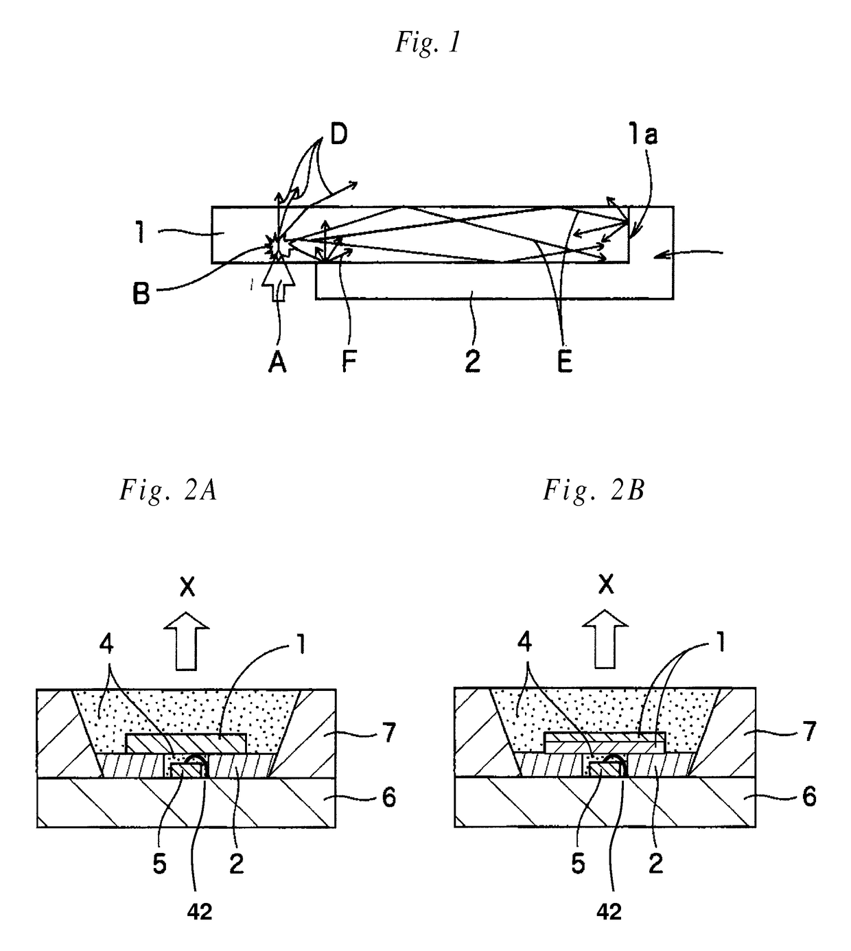
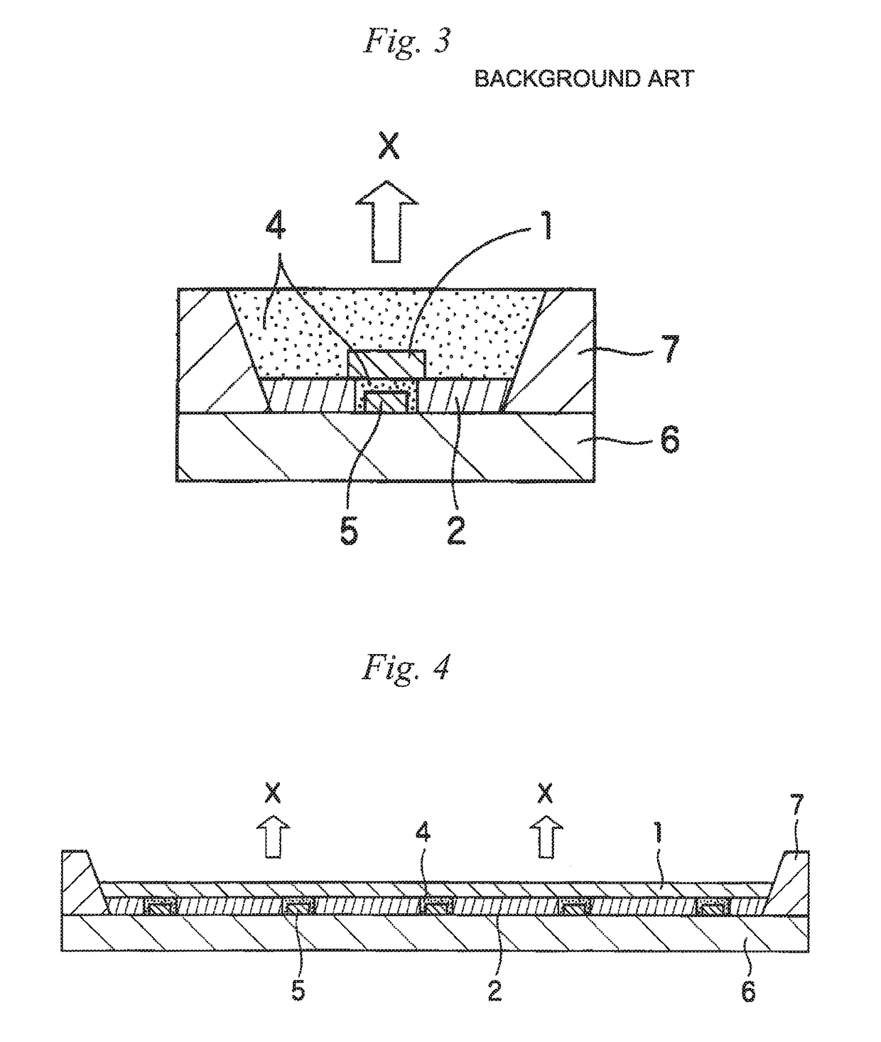
[0036]As above, in the semiconductor light emitting device of the invention, the wavelength conversion layer is provided on an upper side of the LED element and a diffusive reflection resin layer is provided in a state that side faces of the LED element are surrounded therewith, and the area at the LED element side of the wavelength conversion layer is at least twice larger by area ratio than the area of light emitting area on the upper surface of the LED element. Therefore, light propagating to a direction other than the extraction direction among the light emitted at the wavelength conversion layer strikes to the diffusive reflection resin layer and is diffusion-reflected to propagate to the extraction direction. Thus, the light propagating to improper directions is repeatedly diffusion-reflected and is course-corrected to the proper direction. Accordingly, most of the light can be finally guided to the light extraction direction. Consequently, since the back scattering light can be reduced and the light extraction efficiency can be remarkably enhanced, the semiconductor light emitting device of the invention shows a high luminance and a high efficiency.
[0037]Moreover, when the wavelength conversion layer is a phosphor plate which includes a translucent ceramic including a polycrystalline sintered body whose sintered density is 99.0% or more, having a total light transmittance of 40% or more in a visible light wavelength region excluding an excitation wavelength region, and having a thickness of 100 to 1,000 μm, the phosphor plate itself does not contain a resin having a low thermal conductivity, so that heat generated in the phosphor is efficiently radiated to a printed wiring board side through the phosphor plate and thus heat radiation properties are improved. In conventional semiconductor light emitting devices, attention is mainly focused on only the viewpoint how to radiate heat generated from an LED. In the invention, since such a heat radiation measure as described above is performed not only the heat generated from the LED but also heat generated from the wavelength conversion layer, the heat radiation properties are excellent and the invention is particularly advantageous for a high output type power LED.
[0038]Furthermore, unevenness in properties of the wavelength conversion layer, which tends to cause emission color fluctuation between products, can be suppressed to the minimum by using a phosphor plate or phosphor sheet having a controlled thickness as the wavelength conversion layer.
[0039]When the diffusive reflection resin layer is formed from a cured material of a resin composition containing a transparent resin and an inorganic filler different in refractive index from the transparent resin, the heat generated from the phosphor is efficiently radiated to the printed wiring board side through the conducting filler added to the transparent resin. Accordingly, since an efficiency decrease of the LED and the phosphor by temperature elevation is suppressed, higher luminance and higher efficiency can be further realized and also durability of the semiconductor light emitting device is improved.

Problems solved by technology

However, since a contrivance is not made with focusing the back scattering light C particularly in the color conversion layer and from the viewpoint of enhancing the extraction efficiency, the effect is restricted.
However, when the transmittance of the wavelength conversion layer 41 is improved and the diffusivity decreases, as shown in FIG. 23, in addition to the back scattering light C, confinement of the light D propagating to the light extraction direction occurs by total internal reflection attributable to the difference in refractive index between the wavelength conversion layer 41 and an outer region thereof, so that the light extraction efficiency cannot be sufficiently improved.

Method used


Image

  • Semiconductor light emitting device
  • Semiconductor light emitting device
  • Semiconductor light emitting device

Examples


embodiment a

[0076]The phosphor plate is obtained by molding the phosphor material into a desired shape and sintering it under heating and is also referred to as a polycrystalline sintered body because of the production method. As the polycrystalline sintered body, for example, translucent ceramics as described in JP-A-11-147757 and JPA-2001-158660 can be employed. The translucent ceramics have already been in practical use as solid laser materials and highly durable housing materials for high-pressure sodium lamp, metal halide lamp, and the like. The translucency can be enhanced by removing light-scattering sources such as voids and impurities remaining in the ceramics. Moreover, in the isotropic crystal materials represented by YAG, since any difference in refractive index owing to crystal orientation is absent, completely transparent and non-scattering translucent ceramics can be obtained even in the case of polycrystalline ceramics, as in the case of a single crystal. Therefore, the phosphor...

embodiment b

[0102]The phosphor sheet is obtained by applying a solution containing the phosphor material dispersed in a binder resin and molding the solution into a sheet. Specifically, a binder resin containing the phosphor material dispersed therein or an organic solvent solution of the resin is applied on a separator (e.g., surface release-treated PET film) in an appropriate thickness by a method such as casting, spin coating, or roll coating and a film forming step of drying at such a temperature that removal of the solvent is possible is carried out, thereby molding a sheet. The temperature for drying the filmed resin or resin solution cannot be categorically determined since the temperature varies depending on the kinds of the resin and the solvent but is preferably from 80 to 150° C., more preferably from 90 to 150° C.

[0103]As the phosphor particles for use in the phosphor sheet, from the viewpoint of the emission efficiency, one having an average particle diameter of 100 nm or more is p...

example 1

[0151]Using the LED element (four-blue-LEDs mounted type) shown in FIG. 13, an LED element for test was prepared. Namely, first, for the purpose of protecting respective four pieces of the LED chips including wire bonding with the gold wire, a minute amount of a thermosetting silicone elastomer (item No. KER 2500 manufactured by Shin-Etsu Silicone) was attached using a tip of a toothpick and temporarily cured at 100° C. for 15 min. Then, the resin composition for diffusive reflection resin layer formation prepared previously was formed over the whole inner surface (10 mm×10 mm) of the glass epoxy flame. On this occasion, care was taken so that the resin composition did not cover the LED chips. Thereafter, the resin composition was cured by heating at 100° C. for 1 hour and at 150° C. for 1 hour. Then, the silicone elastomer was added dropwise into the glass epoxy flame and a YAG plate diced into a size of 10 mm×10 mm was placed thereon with care so that no air bubbles remained, and ...


PUM


Abstract

The present invention relates to a semiconductor light emitting device including: a substrate for element mounting; a wiring provided on the substrate; an LED element provided on the substrate and electrically connected to the wiring; an encapsulating resin layer for encapsulating the LED element; and a wavelength conversion layer which contains a phosphor material and converts a wavelength of light emitted by the LED element, in which the wavelength conversion layer is provided on an upper side of the LED element, and a diffusive reflection resin layer is provided in a state that side faces of the LED element are surrounded therewith, and an area at the LED element face side of the wavelength conversion layer is at least twice larger by area ratio than an area of light emitting area on an upper surface of the LED element.

Description

CROSS REFERENCE TO RELATED APPLICATIONS[0001]The present application is based on Japanese Patent Application No. 2010-141215 filed on Jun. 22, 2010, and the contents are incorporated herein by reference.[0002]All references cited herein are incorporated by reference herein in their entirety.[0003]Also, all references cited herein are incorporated as a whole.FIELD OF THE INVENTION[0004]The present invention relates to a semiconductor light emitting device. More particularly, it relates to a semiconductor light emitting device having a light emitting diode (LED), particularly a blue LED or a near-ultraviolet LED, that converts the wavelength of a part or all of emission of the LED to emit white light or other visible light.BACKGROUND OF THE INVENTION[0005]As one of visible light sources for displaying or lighting, there is a light emitting device using a blue LED or a near-ultraviolet LED based on a gallium nitride-based compound semiconductor such as GaN, GaAlN, InGaN, or InAlGaN. In...

Claims


Application Information

Patent Timeline
Patent Type & Authority Patents(United States)
IPC IPC(8): H01L29/18H01L33/00H01L33/54H01L33/50
CPCH01L33/54H01L33/505H01L33/507H01L2224/45144H01L2224/48091H01L2224/48247H01L2224/73265H01L2224/8592H01L2924/00014H01L2924/00H01L33/50H01L33/52
Inventor ITO, HISATAKANAKAMURA, TOSHITAKAFUJII, HIRONAKA
Owner SCHOTT AG
Why Eureka
Try Eureka