NAND flash memory device with oblique architecture and memory cell array

a memory cell array and oblique architecture technology, applied in the field of memory devices, can solve the problems of excessive close threshold voltage distribution, increase in the distribution width of threshold voltage, and reduction of read window, and achieve the effect of reducing the capacitance of adjacent memory cells

Active Publication Date: 2017-04-04
MACRONIX INT CO LTD
View PDF7 Cites 0 Cited by
  • Summary
  • Abstract
  • Description
  • Claims
  • Application Information

AI Technical Summary

Benefits of technology

[0008]The invention is directed to a memory device, in which a coupling capacitance between adjacent memory cells is decrease

Problems solved by technology

As a gap between word lines is reduced, a space between floating gates of unit cells is also compressed, such that the adjacent cells may interfere with each other to cause a drift of a threshold voltage (Vth), and such interference results in a fact that a distribution width of the threshold voltage is increased.
When a line width of the memory is reduced to be smaller than 2× nanome

Method used


Image

  • NAND flash memory device with oblique architecture and memory cell array
  • NAND flash memory device with oblique architecture and memory cell array
  • NAND flash memory device with oblique architecture and memory cell array

Examples


Embodiment Construction

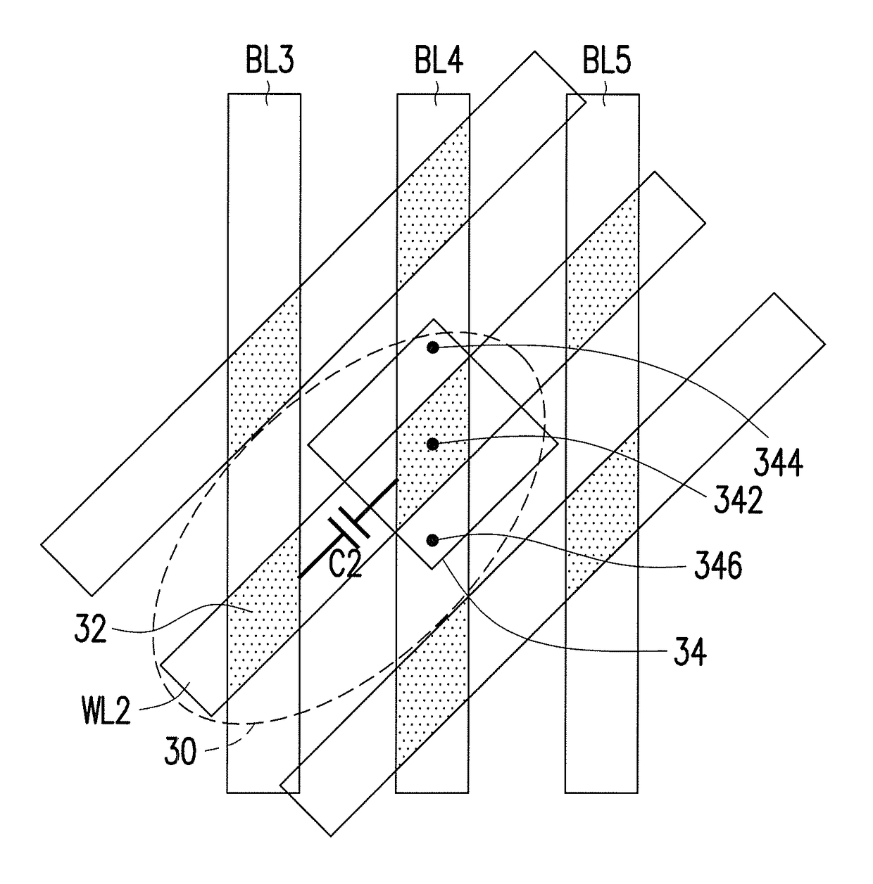
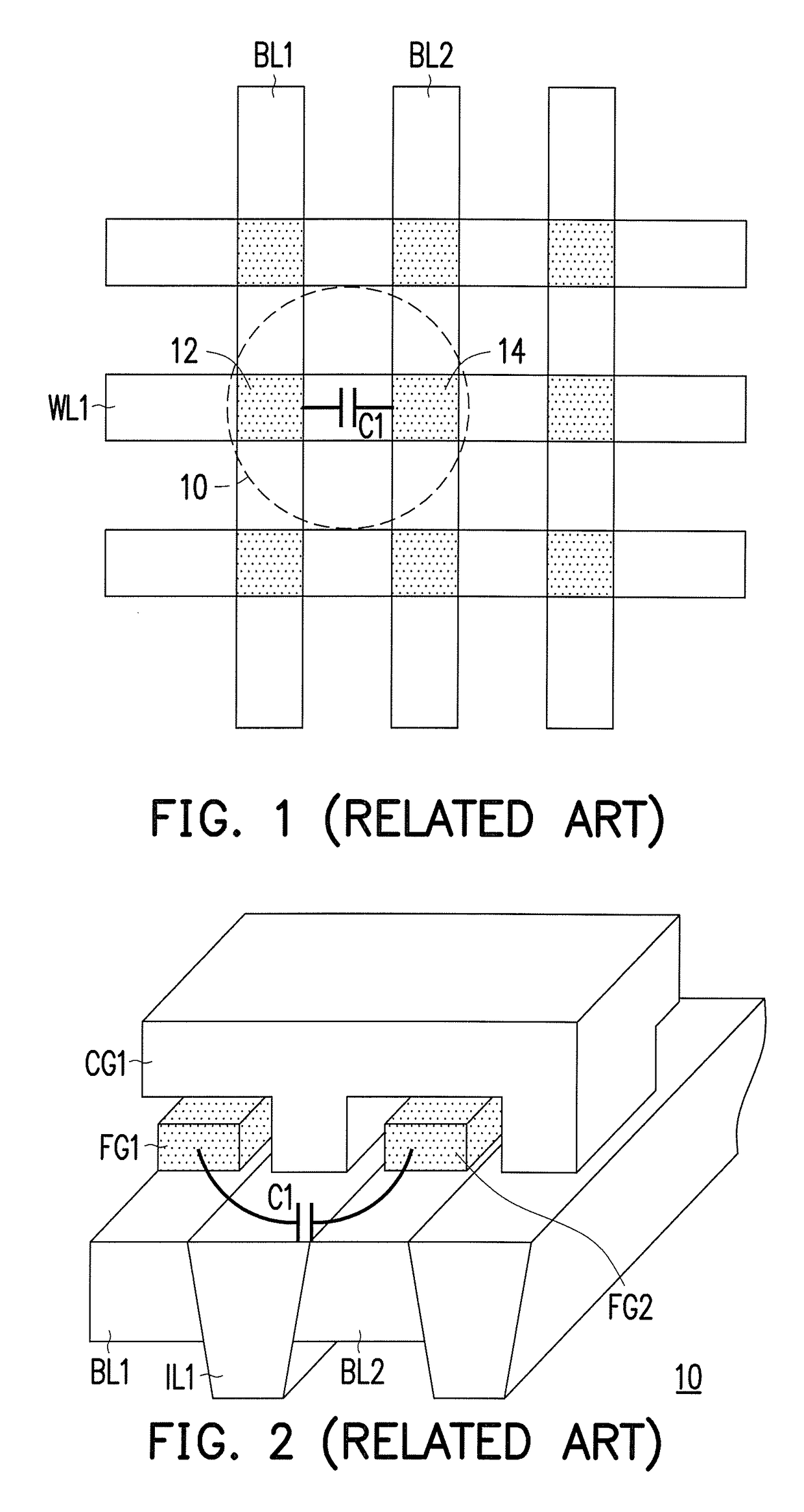
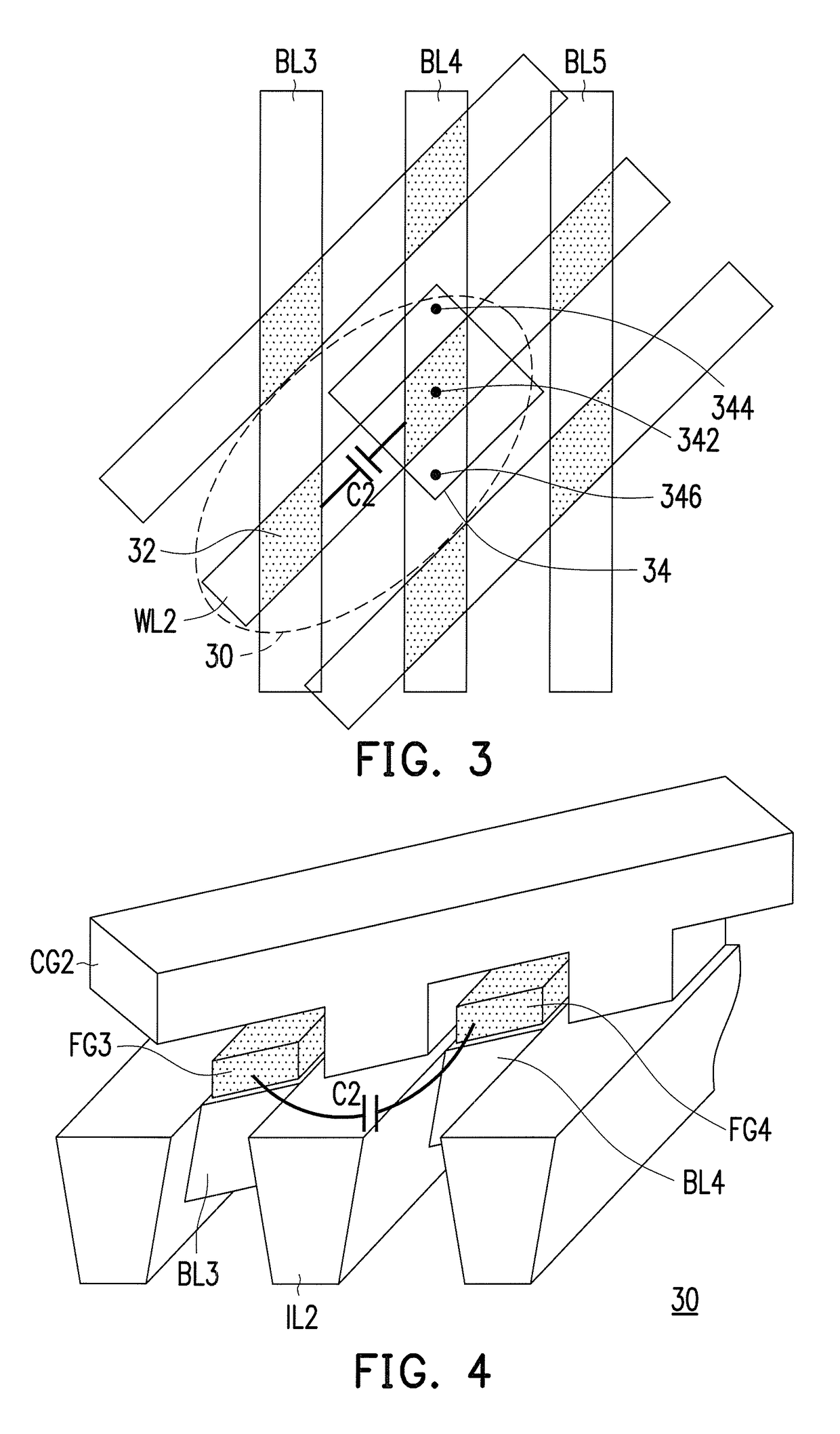
[0032]In a NAND flash memory of the invention, an original perpendicular configuration between word lines and bit lines is changed to an oblique configuration, such that floating gate regions of two adjacent memory cells are staggered along a bit line direction. In this way, an overlapping width between the floating gate regions of the adjacent memory cells is decreased to reduce a coupling capacitance formed therebetween, so as to mitigate a bit line to bit line interference.

[0033]FIG. 3 is a layout schematic diagram of a memory device according to an embodiment of the invention. The memory device of the present embodiment includes a plurality of word lines parallel to each other (for example, a word line WL2 in FIG. 3) in a first direction, a plurality of bit lines parallel to each other (for example, bit lines BL3, BL4, BL5 in FIG. 3) in a second direction, where the bit lines respectively intersect the word lines, and an included angle between bit lines and the word lines is not...


PUM


Abstract

A memory device including multiple word lines, multiple bit lines and a memory cell array is provided. The word lines intersect the bit lines, and an included angle between the word lines and the bit lines is not a right angle. The memory cell array includes multiple memory cells respectively disposed at the intersections of the word lines and the bit lines. Each row of the memory cells is electrically connected to one of the word lines, and each column of the memory cells is electrically connected to one of the bit lines.

Description

BACKGROUND OF THE INVENTION[0001]Field of the Invention[0002]The invention relates to a memory device, and particularly relates to a NAND flash memory device.[0003]Description of Related Art[0004]Along with a continuous increase of the number of transistors used in a NAND flash memory, the size of the transistors becomes smaller, and lines for connecting the transistors become denser. As a gap between word lines is reduced, a space between floating gates of unit cells is also compressed, such that the adjacent cells may interfere with each other to cause a drift of a threshold voltage (Vth), and such interference results in a fact that a distribution width of the threshold voltage is increased.[0005]When a line width of the memory is reduced to be smaller than 2× nanometers (nm), a bit line direct interference becomes more important, especially the interference from the floating gate to an adjacent channel on a bit line direction may cause a reduction of a read window. Therefore, th...

Claims


Application Information

Patent Timeline
IPC IPC(8): G11C11/34G11C11/418G11C16/08G11C16/24G11C16/04
CPCG11C16/08G11C11/418G11C16/24G11C16/0408G11C5/05G11C5/063G11C16/0483H10B41/10H10B41/35
Inventor LEE, YA-JUICHEN, KUAN-FU
Owner MACRONIX INT CO LTD
Why Eureka
Try Eureka