Array substrate and manufacturing method thereof, and display apparatus

a technology applied in the field of array substrate and manufacturing method thereof, can solve the problems of poor display on the display apparatus, high production cost, etc., and achieve the effect of improving the display quality

Inactive Publication Date: 2018-03-06
BOE TECH GRP CO LTD +1
View PDF13 Cites 0 Cited by
  • Summary
  • Abstract
  • Description
  • Claims
  • Application Information

AI Technical Summary

Benefits of technology

[0005]With respect to poor displays due to the large coupling capacitance between the pixel electrode and the data line of the existing array substrate, the invention provides an array substrate and manufacturing method thereof, and a display apparatus comprising the array substrate, which can reduce the coupling capacitance between the data line and the pixel electrode of the array substrate, thereby the poor displays can be improved.
[0007]In the manufacturing method of an array substrate according to the present invention, the data line layer is first formed on the substrate, thus the distance between the data line layer and the pixel electrode becomes larger, and the coupling capacitance between the data line and the pixel electrode is reduced, thereby the poor displays due to the large coupling capacitance between the pixel electrode and the data line are avoided, and the quality of the displays are improved.
[0023]In the array substrate of the present invention, the data line is below the active layer, resulting in an increased distance between the layer of the data line and the pixel electrode, thereby the coupling capacitance between the data line and the pixel electrode is reduced, and the poor displays due to the large coupling capacitance are improved.
[0025]As the display apparatus of the present invention comprises the above array substrate, the display quality thereof is improved.

Problems solved by technology

The inventor of the present invention finds that, there are at least following problems in the prior art: with respect to the existing array substrate comprising a LTPS thin film transistor, the manufacturing process thereof is complex, the cost of production is high, and the distance between the layer of the data line and the layer of the pixel electrode is small and the edge of the pixel electrode overlaps with the data line, thus a large coupling capacitance is produced between the pixel electrode and the data line, resulting in a transmission delay of the signal on the data line, which influences the distribution of the liquid crystal molecules around the pixel electrode, in turn, can lead to poor displays on the display apparatus comprising the array substrate, for example, vertical moirés in lumps are generated in the pictures displayed on the display apparatus.

Method used


Image

  • Array substrate and manufacturing method thereof, and display apparatus
  • Array substrate and manufacturing method thereof, and display apparatus
  • Array substrate and manufacturing method thereof, and display apparatus

Examples


embodiment 1

[0035

[0036]The present embodiment provides a manufacturing method of an array substrate. Referring to FIGS. 4-6, the manufacturing method comprises the following steps.

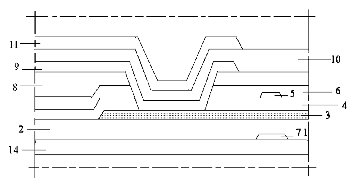
[0037]S1, depositing a data line metal layer on a substrate 14 by sputtering, thermal evaporation method, or other film forming methods, and forming a pattern of a data line 7 by a patterning process. The substrate 14 may be a glass substrate or other types of transparent substrate, and the data line metal layer may be formed of one of chromium (Cr), molybdenum (Mo), aluminum (Al), copper (Cu), tungsten (W), neodymium (Nd), or formed of an alloy of them. Moreover, the data line metal layer may be of one layer or more than one layers.

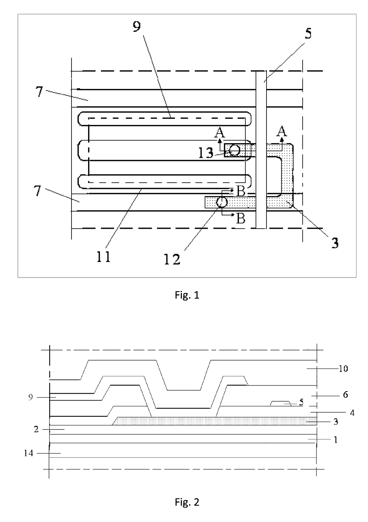
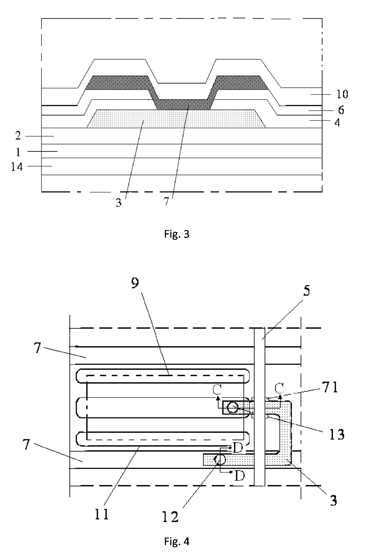
[0038]S2, forming a semiconductor layer on the substrate 14 formed with the data line 7 thereon, and forming a pattern of an active layer 3 by a patterning process, wherein the data line 7 is connected with the active layer 3.

[0039]The step S2 further comprises: depositing a polycrystallin...

embodiment 2

[0059

[0060]The present embodiment provides an array substrate. As shown in FIG. 4 to FIG. 8, the array substrate comprises a data line 7 and an active layer 3, wherein the data line 7 is below the active layer 3, and the data line 7 is connected with the active layer 3. Of course, the array substrate further comprises some known structures such as a gate line 5, a pixel electrode and so on, which are not described here.

[0061]The array substrate further comprises a pattern 71 of a shield metal for shielding the active region of the active layer 3, and the pattern 71 of the shield metal is below the active layer 3. As the active layer 3 is a semiconductor layer formed of polycrystalline silicon, and the semiconductor material is photosensitive, when it is irradiated by light (such as light from a backlight module), a leakage current may be generated therein, which influences performances of the active layer 3, and there may be adverse impacts on the performances of the thin film trans...


PUM


Abstract

The present invention provides an array substrate and a manufacturing method thereof, and a display apparatus comprising the array substrate an array substrate, which can avoid poor displays due to large coupling capacitance between a data line and a pixel electrode in an array substrate in the prior art. The manufacturing method comprises the following steps: S1, forming a data line metal layer on a substrate, and forming a pattern of a data line by a patterning process; S2, forming a semiconductor layer on the substrate formed with the data line thereon, and forming a pattern of an active layer by a patterning process, wherein the data line is connected with the active layer.

Description

FIELD OF THE INVENTION[0001]The present invention relates to the field of display technology, and particularly, to an array substrate and manufacturing method thereof, and a display apparatus comprising the array substrate.BACKGROUND OF THE INVENTION[0002]In the field of display technology, a thin film transistor is usually used as a switching element for controlling operations of a pixel unit. According to characteristics of silicon thin films in active layer of thin film transistor, thin film transistors can be classified into two types of amorphous silicon (a-Si) thin film transistors and polycrystalline silicon (poly-Si) thin film transistors. Amorphous silicon thin film transistors have defects such as low on-state current, low electronic mobility, poor stability, etc., and polycrystalline silicon thin film transistors have superior performances such as high electronic mobility, low leakage current, and so on. Therefore, a display apparatus with polycrystalline silicon thin fil...

Claims


Application Information

Patent Timeline
Patent Type & Authority Patents(United States)
IPC IPC(8): H01L27/12
CPCH01L27/124H01L27/127
Inventor CHEN, YONGMO, ZAILONGSHI, TIANLEIPARK, SEUNGYIK
Owner BOE TECH GRP CO LTD
Why Eureka
Try Eureka