Liquid crystal display and fabricating method thereof

a technology of liquid crystal display and fabrication method, which is applied in the field of liquid crystal display, can solve the problems of affecting yield, deteriorating display quality, and weakening signals, and achieve the effect of reducing crosstalk and ameliorating display quality problems

Inactive Publication Date: 2007-07-24
INNOLUX CORP
View PDF3 Cites 0 Cited by
  • Summary
  • Abstract
  • Description
  • Claims
  • Application Information

AI Technical Summary

Benefits of technology

[0014]Accordingly, an object of the present invention is to reduce crosstalk, thereby ameliorating display quality problems.
[0015]Therefore, in the invention, the pixel electrode layer on the color filter substrate is thinned or removed above the signal lines on the TFT array substrate to reduce coupling capacitance between the pixel electrode on the color filter substrate and the signal lines on the TFT array substrate, reducing crosstalk, improving display quality, and increasing performance and yield.
[0020]The relatively thin part of the second pixel electrode layer is formed by, for example, photolithography to thin or remove the corresponding part of the pixel electrode layer, such that a thinned part, thinner than the pixel electrode layer, or a hollow part, is formed. The thickness of the thinned part is not limited. As long as the part is thinned, i.e. thinner than the other part of the pixel electrode layer, the coupling capacitance between the pixel electrode layer and the signal lines can be reduced, such that the object of the invention can be fulfilled. Accordingly, thickness of the thinned part is preferably zero, such that the pixel electrode in the area is preferably completely removed to be hollow.
[0022]According to the inventive liquid crystal display and fabricating method thereof, capacitance loading of the signal lines is reduced by thinning of the corresponding pixel electrode, such that crosstalk resulting from coupling capacitance is reduced, and display quality is improved.

Problems solved by technology

Two layers of metal with dielectric material, i.e. the liquid crystal layer 3, inserted therebetween, result in capacitor effect, which weakens the signals, produces crosstalk, deteriorating display quality and affecting yield.
Moreover, crosstalk becomes more serious in larger display panels.

Method used


Image

  • Liquid crystal display and fabricating method thereof
  • Liquid crystal display and fabricating method thereof
  • Liquid crystal display and fabricating method thereof

Examples


Embodiment Construction

Manufacture of TFT Array Substrate

[0031]FIGS. 6A-6D show the manufacturing process of TFT array substrate of the invention. Bottom-gate type TFT is used here to explain the manufacturing process, while top-gate type TFT is also applicable.

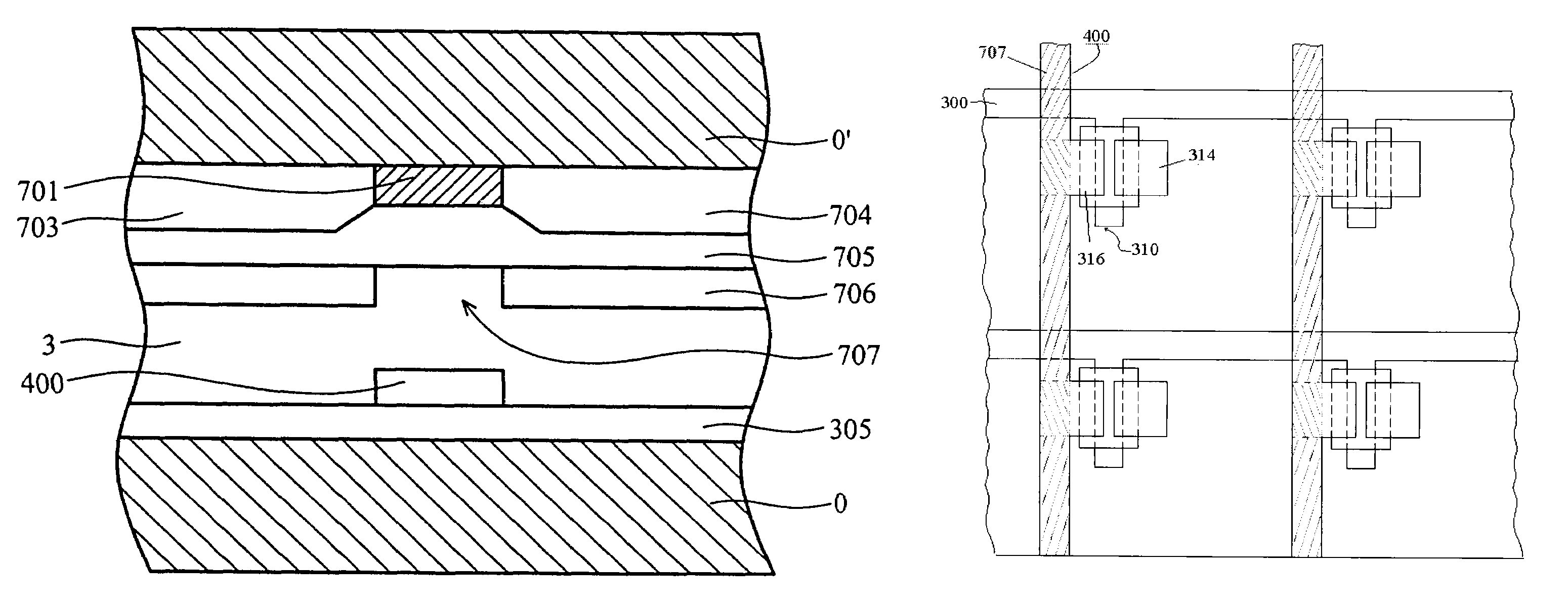
[0032]First, as in FIG. 6A, a substrate 0 of, for example, glass, is provided. A deposition step is performed thereon, followed by a first photolithography step, to form parallel gate lines 300, 301 in a row direction on the substrate 0, wherein the gate line 300 has a protruding part, which is the gate electrode 312. Next, a gate insulating layer 305 (not shown) is formed on the gate lines 300, 301, gate electrode 312 and the substrate 0. The gate lines 300, 301 and gate electrode 312 are metal, formed by, for example, deposition. The gate insulating layer 305 is, for example, SiO2, SiNx, or silicon oxynitride, formed by deposition.

[0033]In FIG. 6B, a deposition step is performed on the substrate, followed by a second photolithography step, to for...


PUM

PropertyMeasurementUnit
cross-sectionaaaaaaaaaa
sizesaaaaaaaaaa
yieldaaaaaaaaaa

Abstract

A liquid crystal display (LCD) and fabricating method thereof. The LCD includes a first substrate, provided with a plurality of parallel gate lines and a plurality of parallel signal lines, wherein the gate lines and signal lines are perpendicular, and a pixel area is defined by two adjacent gate lines and two adjacent signal lines. A source electrode, electrically connected to one of the adjacent signal lines, and a drain electrode are formed on the pixel area. A first pixel electrode is formed, electrically connected to the drain electrode, on the pixel area. A second substrate is provided a predetermined distance above the first substrate, having a plurality of color-filtering areas, directly above the respective pixel area. A second pixel electrode layer is formed on the second substrate, wherein the part thereof directly above the signal lines is relatively thin.

Description

[0001]This application is a divisional of U.S. application Ser. No. 10 / 436,795, filed May 13, 2003 U.S. Pat. No. 6,965,423.BACKGROUND OF THE INVENTION[0002]1. Field of the Invention[0003]The present invention relates to a liquid crystal display, and more particularly to a liquid crystal display with reduced crosstalk.[0004]2. Description of the Related Art[0005]Liquid crystal display (LCD) is a commonly used flat panel display. Owing to dielectric anisotropy and conductive anisotropy of liquid crystal molecules, molecular orientation of liquid crystals can be shifted under an external electronic field, such that various optical effects are produced.[0006]A LCD panel is generally made up of two substrates, with a certain gap preserved therebetween, and a liquid crystal layer filled within the gap. Respective electrodes are formed on the two substrates, respectively, to control the orientation and oriental shift of liquid crystal molecules.[0007]A TFT (thin film transistor) LCD panel ...

Claims


Application Information

Patent Timeline
Patent Type & Authority Patents(United States)
IPC IPC(8): G02F1/1343G02F1/1335G02F1/1333G02F1/136H01L21/00
CPCG02F1/134309G02F1/133345
Inventor CHEN, JUN CHANGTAI, YA-HSIANG
Owner INNOLUX CORP
Why Eureka
Try Eureka