Check patentability & draft patents in minutes with Patsnap Eureka AI!

Gate pulse modulation waveform-shaping circuit

a waveform-shaping circuit and gate technology, applied in pulse manipulation, pulse technique, electrical equipment, etc., can solve the problems of different brightness at left and right sides of frames, material preparation problems, overheating of ics

Active Publication Date: 2017-04-11
INNOLUX CORP
View PDF4 Cites 0 Cited by
  • Summary
  • Abstract
  • Description
  • Claims
  • Application Information

AI Technical Summary

Benefits of technology

The patent is about a circuit that can change the voltage waveform of a signal on a scan line using a resistor. This helps to reduce the difference in brightness between different parts of a frame. It also prevents overheating of the circuit by avoiding the use of a resistor in the IC.

Problems solved by technology

Due to the resistance-capacitance (RC) load effect, signal on the scan line which is distant from the gate driver may present a dragging situation, so that the waveform of the signal on the scan line which is close to the gate driver is quite different from that distant from the gate driver, resulting in that the brightness at left and right sides of a frame is different.
However, because different LCD panels require different slopes, the value of the resistance R has to be adjusted to satisfy the actual requirement, which may cause a material preparation problem on production as different types of LCD panels require different resistance values.
However, such a way to implement the resistor in the IC may overheat the IC, and even burn down the IC.

Method used


Image

  • Gate pulse modulation waveform-shaping circuit
  • Gate pulse modulation waveform-shaping circuit
  • Gate pulse modulation waveform-shaping circuit

Examples


Embodiment Construction

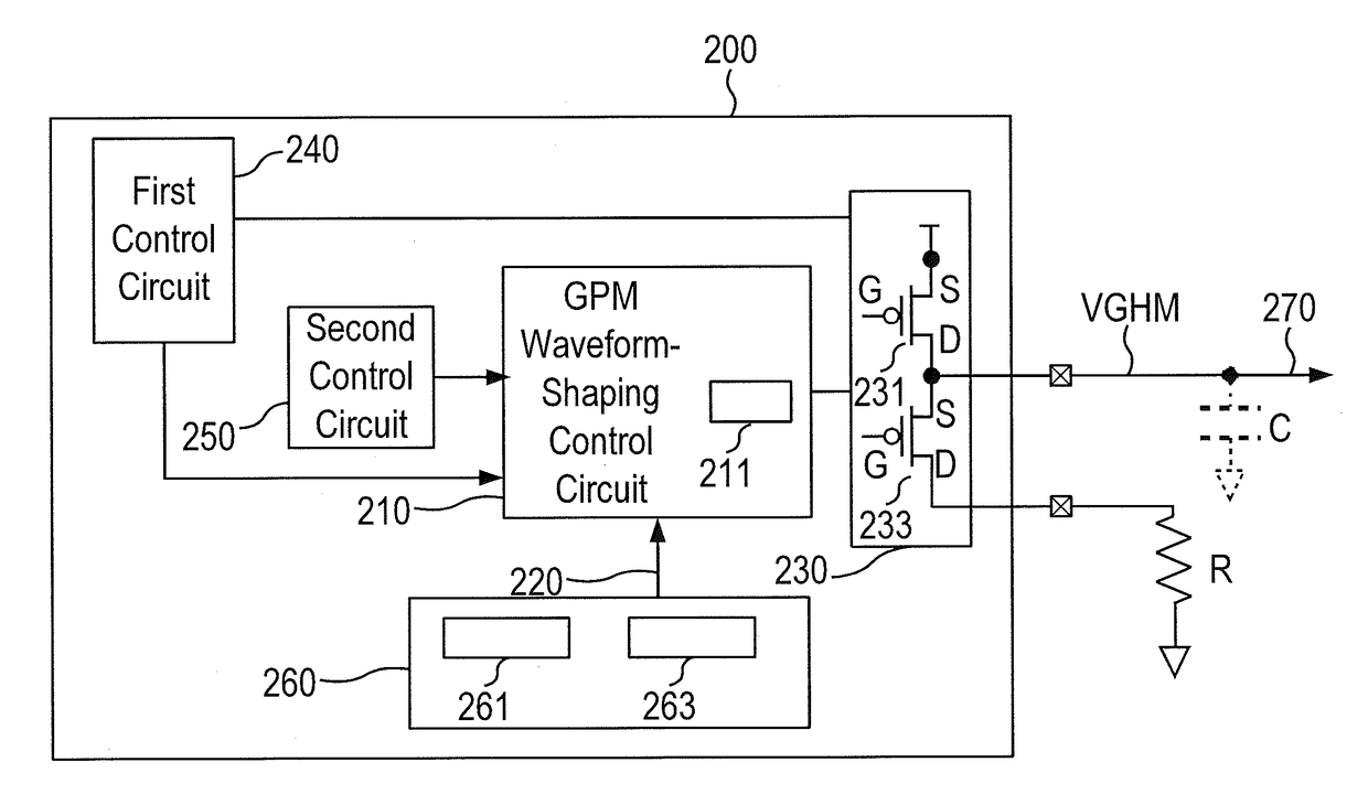
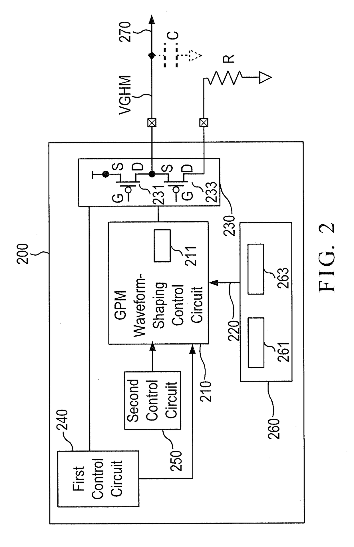
[0022]FIG. 2 is a block diagram of a gate pulse modulation waveform-shaping circuit 200 in accordance with the invention. The gate pulse modulation waveform-shaping circuit 200 includes a gate pulse modulation waveform-shaping control circuit 210, an input terminal 220, an output pair 230, a first control circuit 240, a second control circuit 250, and a delay parameter circuit 260.

[0023]The input terminal 220 is employed to receive a control signal. The control signal is provided by the delay parameter circuit 260. The output pair 230 is connected to a scan line 270 for outputting a gate output voltage. The output pair 230 has a first PMOS transistor 231 and a second PMOS transistor 233.

[0024]The first PMOS transistor 231 has a source connected to a high voltage and a drain connected to the scan line 270 and a source of the second PMOS transistor 233. The second PMOS transistor 233 has a drain connected to an external resistance R.

[0025]The gate pulse modulation waveform-shaping con...


PUM


Abstract

A gate pulse modulation waveform-shaping circuit includes an input terminal, an output pair, and a gate pulse modulation waveform-shaping control circuit. The input terminal receives a control signal. The output pair is connected to a scan line for outputting a gate output voltage. The gate pulse modulation waveform-shaping control circuit is connected to the output pair for adjusting a voltage waveform on the scan line. The gate pulse modulation waveform-shaping control circuit is based on the control signal to use a time interval or fixed discharge voltage to generate a desired delay for adjusting a discharge slope thereby generating different discharge time on the scan line, so that the gate output voltage has a voltage waveform including at least two waveform segments each with a non-zero sliding slope and at least two waveform segments each with a zero slope.

Description

BACKGROUND OF THE INVENTION[0001]1. Field of the Invention[0002]The present invention relates to the technical field of LCD devices and, more particularly, to a gate pulse modulation waveform-shaping circuit.[0003]2. Description of Related Art[0004]Currently, the liquid crystal display (LCD) is the most common flat display device, which has the advantages of compactness, low power consumption, and low radiation. The operating principle of LCD is to regulate the voltage difference between two ends of a liquid crystal layer to change the arrangement of liquid crystal molecules in the liquid crystal layer thereby changing the transmittance of the liquid crystal layer, and to further make use of a light source provided by a backlight module to display an image.[0005]The LCD device includes a plurality of pixel units, a source driver, and a gate driver. The source driver provides a plurality of data signals to the plurality of pixel units. The gate driver generates a plurality of gate si...

Claims


Application Information

Patent Timeline
Patent Type & Authority Patents(United States)
IPC IPC(8): H03K7/08
CPCH03K7/08H03K5/12
Inventor SHIH, CHING-WENHUANG, FU-HSIEN
Owner INNOLUX CORP
Features
  • R&D
  • Intellectual Property
  • Life Sciences
  • Materials
  • Tech Scout
  • Unparalleled Data Quality
  • Higher Quality Content
  • 60% Fewer Hallucinations
Learn More