Liquid crystal display panel and liquid crystal display device containing the same

a liquid crystal display panel and liquid crystal display technology, which is applied in non-linear optics, instruments, optics, etc., can solve the problems of unsatisfactory alignment of liquid crystal molecules, and achieve the effect of improving the display quality of the liquid crystal display panel

Active Publication Date: 2017-04-25
INNOLUX CORP
View PDF22 Cites 6 Cited by
  • Summary
  • Abstract
  • Description
  • Claims
  • Application Information

AI Technical Summary

Benefits of technology

[0008]An object of the present invention is to provide a liquid crystal display panel and a liquid crystal display device containing the same, which can solve the problem of disclinations of liquid crystal molecules to improve the display quality of the liquid crystal display panel and the device containing the same.
[0011]In general, several kinds of elements having different heights are laminated on the first substrate of the liquid crystal panel. In the liquid crystal display panel of the present invention, although the distances between the second surface of the first alignment layer and the first surface of the first substrate (in short, the distance between the first alignment layer and the first substrate) in the second region and the third region are different, the altitude difference of the third surface of the first alignment layer in the second region and the third region can be minimized by adjusting the thickness of the first alignment layer; and therefore, the problem of non-uniform rubbing or monomer aggregation of the alignment layer can be prevented to improve the display quality of the liquid crystal display panel. Particularly, the distances between the third surface of the first alignment layer and the first surface of the first substrate in the second region and the third region are different, and the distance difference between the second region and the third region can be greatly reduced by adjusting the thickness of the first alignment layer, in the liquid crystal display panel of the present aspect of the present invention.
[0016]Generally, the thickness of the data line or / and the scan line is larger than that of the pixel electrode in the liquid crystal display panel. Hence, in the liquid crystal display panel of the present invention, the first thickness of the first alignment layer on the pixel electrode (particularly, the pixel electrode in the aperture region of the pixel electrode region) is designed to be larger than the second thickness thereof on the data line and / or the scan line, so the altitude difference of the surface of the first alignment layer on the pixel region and the data line or / and the scan line can be reduced. Therefore, the problem of non-uniform rubbing or monomer aggregation of the alignment layer can be prevented to improve the display quality of the liquid crystal display panel.
[0028]In addition, in the liquid crystal display panel and the method for manufacturing the same of the present invention, a sealant is used to assemble the first substrate and the second substrate. Hence, the liquid crystal display panel of the present invention may further comprise a sealant disposed between the first substrate and the second substrate, and selectively covering parts of the alignment layer. More specifically, the sealant selectively covers the periphery region of the alignment layer. When the protrusion and / or the hump are formed on the alignment layer, the sealant preferably covers parts of the protrusion and / or the hump. The disposition of the protrusion and / or the hump can increase the contact area between the sealant and the alignment layer, and therefore the peeling problem of the sealant from the alignment layer can be improved.

Problems solved by technology

This altitude difference may cause the problem of non-uniform rubbing or monomer aggregation of the alignment layer, resulting in the alignment of the liquid crystal molecules not ideal enough.

Method used


Image

  • Liquid crystal display panel and liquid crystal display device containing the same
  • Liquid crystal display panel and liquid crystal display device containing the same
  • Liquid crystal display panel and liquid crystal display device containing the same

Examples


Embodiment Construction

[0043]The present invention has been described in an illustrative manner, and it is to be understood that the terminology used is intended to be in the nature of description rather than of limitation. Many modifications and variations of the present invention are possible in light of the above teachings. Therefore, it is to be understood that within the scope of the appended claims, the invention may be practiced otherwise than as specifically described.

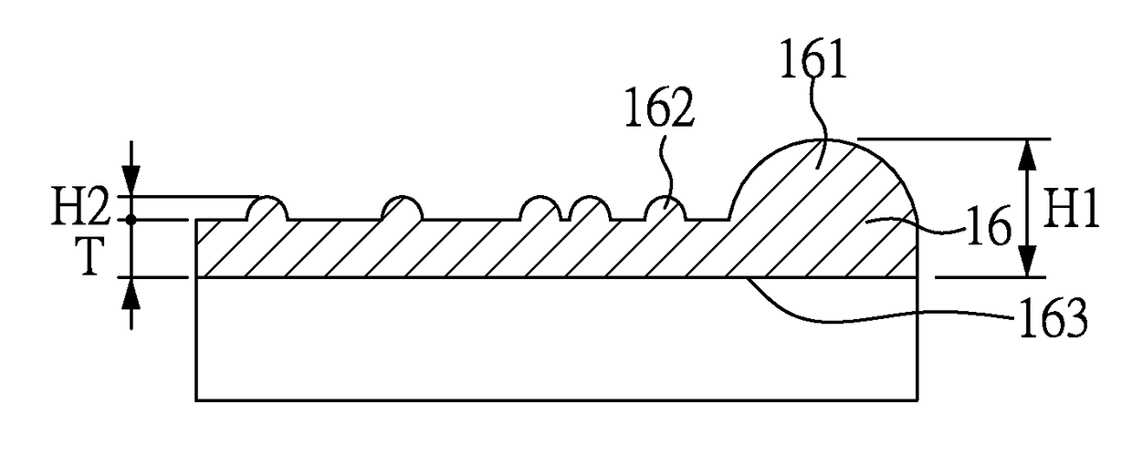
[0044]FIG. 1 is a perspective view of a liquid crystal panel according to one preferred embodiment of the present invention. The liquid crystal display panel of the present embodiment is a liquid crystal display panel configured with a color filter on array (COA) structure, which comprises: a first substrate 11, a second substrate 21, plural spacers 3, a liquid crystal layer 4 and a sealant 5. The first substrate 11 and the second substrate 21 are opposite to each other, the spacers 3 and the liquid crystal layer 4 are disposed betwe...


PUM

PropertyMeasurementUnit
thicknessaaaaaaaaaa
heightaaaaaaaaaa
thickness T2aaaaaaaaaa

Abstract

A liquid crystal display panel and a liquid crystal display device containing the same are disclosed. The liquid crystal display panel of the present invention comprises: a first substrate with a pixel electrode region and a non-pixel electrode region; a second substrate opposite to the first substrate; a first alignment layer disposed on the pixel electrode region and the non-pixel electrode region; and a liquid crystal layer disposed between the first substrate and the second substrate. Herein, the first alignment layer on the pixel electrode region has a first thickness, that on the non-pixel electrode region has a second thickness, and the first thickness is larger than the second thickness.

Description

BACKGROUND OF THE INVENTION[0001]1. Field of the Invention[0002]The present invention relates to a liquid crystal display panel and a liquid crystal display device containing the same and, more particularly, to a liquid crystal display panel with novel structured alignment layers and a liquid crystal display device containing the same.[0003]2. Description of Related Art[0004]In recent years, all the display devices are developed toward having small volume, thin thickness and light weight as the display techniques progresses. A liquid crystal display (LCD) device is a flat panel display device with a thin thickness, so a conventional cathode ray tube (CRT) display is gradually replaced by the LCD. Especially, the LCD can be applied to various fields. For example, the daily used devices such as cell phones, notebooks, video cameras, cameras, music players, navigation devices, and televisions are equipped with liquid crystal display (LCD) panels.[0005]The brightness, the contrast, the ...

Claims


Application Information

Patent Timeline
Patent Type & Authority Patents(United States)
IPC IPC(8): G02F1/1337G02F1/1339G02F1/1333
CPCG02F1/133784G02F1/1339G02F2001/133388G02F1/133388G02F1/133512G02F1/133707G02F1/13394G02F1/134309G02F1/136286G02F1/1368G02F2201/123G02F1/133776G02F1/136222
Inventor CHIU, CHANG-RUCHU, HSIA-CHINGLIN, FENG-LINCHEN, LI-CHUNCHEN, FU-CHENG
Owner INNOLUX CORP
Why Eureka
Try Eureka