Methods, apparatus and system for providing source-drain epitaxy layer with lateral over-growth suppression

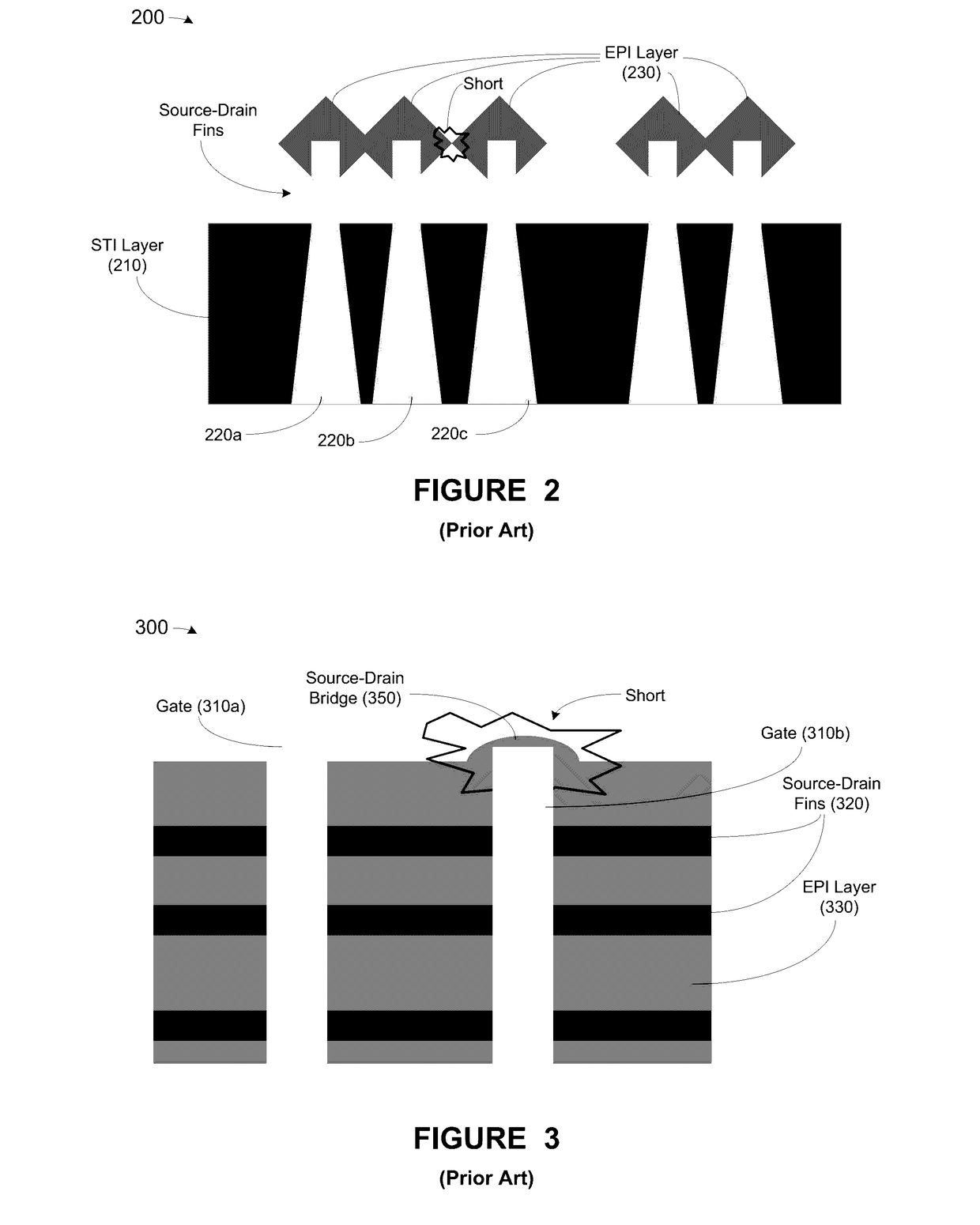
a technology of epitaxy layer and drain region, which is applied in the field of high-performance finfet devices using epitaxial layer with overgrowth suppression, can solve the problems of reducing the channel length of a fet, reducing the distance between the source region and the drain region, and difficult to efficiently inhibit the electrical potential of the channel from being adversely affected

US9640533B2Active Publication Date: 2017-05-02GLOBALFOUNDRIES U S INC
3 Cites 11 Cited by

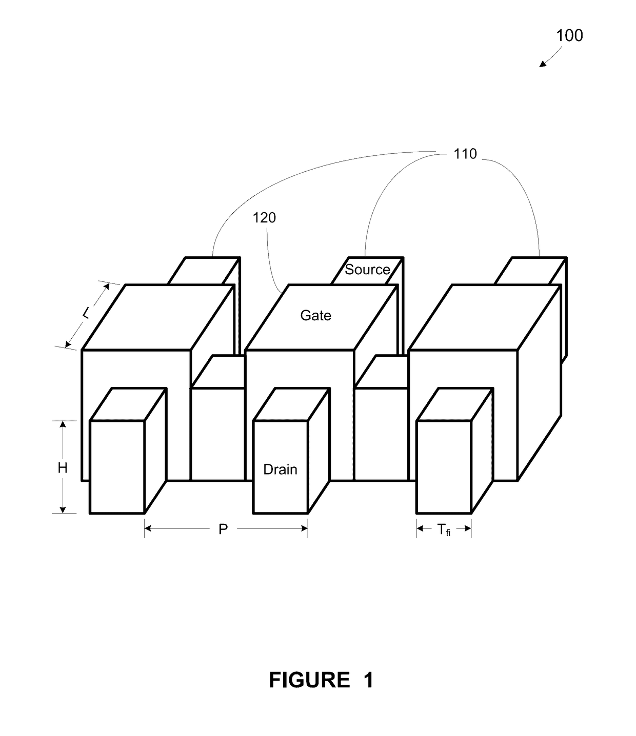
Patent Information

Authority / Receiving Office
US · United States
Patent Type
Patents(United States)
Current Assignee / Owner
Publication Date
2017-05-02

Smart Images

  • Figure 1
    Figure 1
  • Figure 2
    Figure 2
  • Figure 3
    Figure 3
Patent Text Reader

Abstract

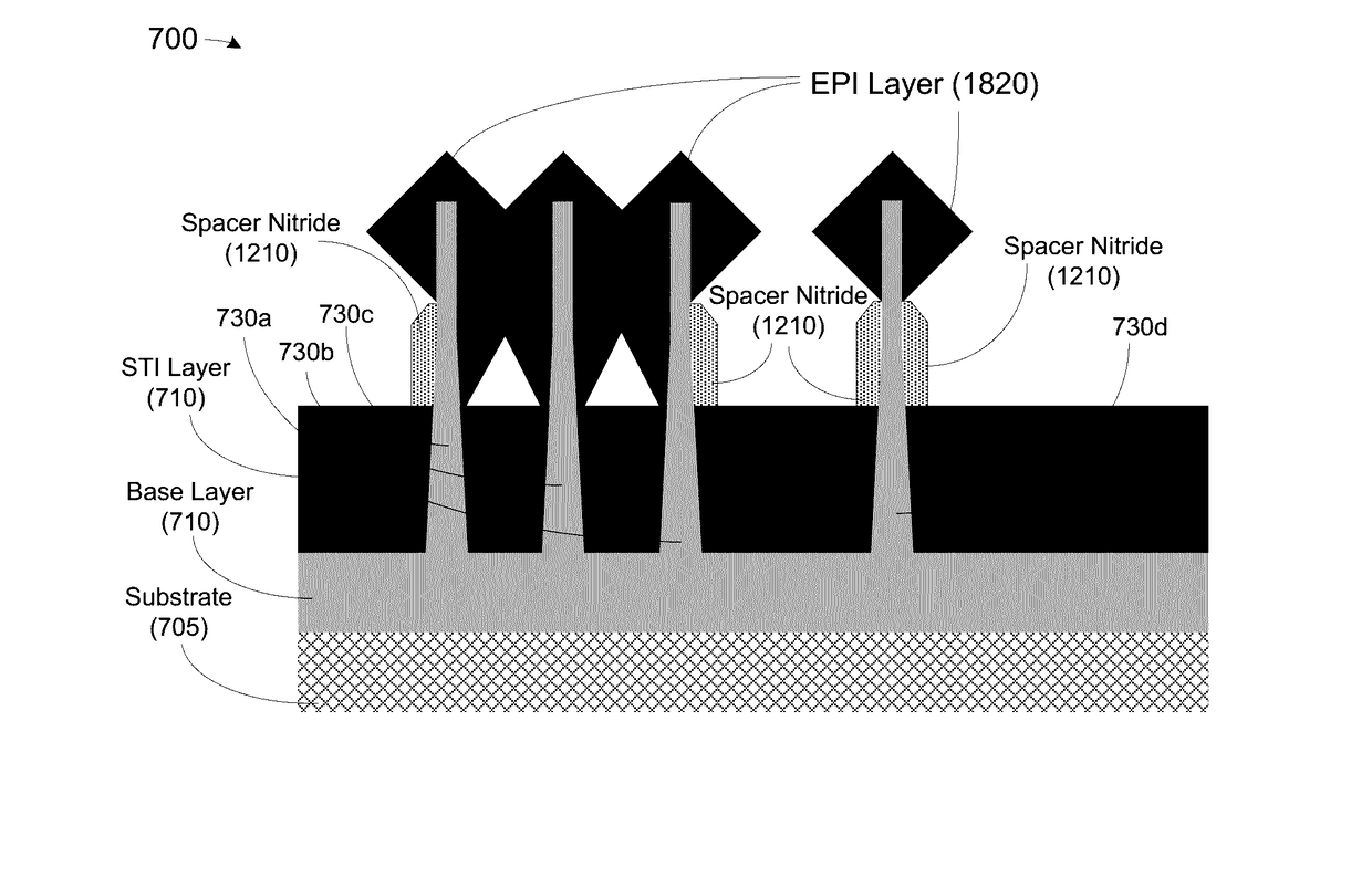
At least one method, apparatus and system disclosed herein for suppressing over-growth of epitaxial layer formed on fins of fin field effect transistor (finFET) to prevent shorts between fins of separate finFET devices. A set of fins of a first transistor is formed. The set of fins comprises a first outer fin, an inner fin, and a second outer fin. An oxide deposition process is performed for depositing an oxide material upon the set of fins. A first recess process is performed for removing a portion of oxide material. This leaves a portion of the oxide material remaining on the inside walls of the first and second outer fins. A spacer nitride deposition process is performed. A spacer nitride removal process is performed, leaving spacer nitride material at the outer walls of the first and second outer fins. A second recess process is performed for removing the oxide material from the inside walls of the first and second outer fins. An epitaxial layer deposition processed upon the set of fins. A portion of the lateral over-growth of epitaxial layer on the outer walls of the first and second outer fins is suppressed by the spacer nitride material.
Need to check novelty before this filing date? Find Prior Art

Description

BACKGROUND OF THE INVENTION

[0001] Field of the Invention

[0002] Generally, the present disclosure relates to the manufacture of sophisticated semiconductor devices, and, more specifically, to various methods for fabricating high performance finFET devices using epitaxial layer with over-growth suppression.

[0003] Description of the Related Art

[0004] The fabrication of advanced integrated circuits, such as CPU's, storage devices, ASIC's (application specific integrated circuits) and the like, requires the formation of a large number of circuit elements in a given chip area according to a specified circuit layout, wherein so-called metal oxide field effect transistors (MOSFETs or FETs) represent one important type of circuit element that substantially determines performance of the integrated circuits. A FET is a device that typically includes a source region, a drain region, a channel region that is positioned between the source region and the drain region, and a gate electrode positioned a...

Examples

Embodiment Construction

[0040]Various illustrative embodiments of the invention are described below. In the interest of clarity, not all features of an actual implementation are described in this specification. It will of course be appreciated that in the development of any such actual embodiment, numerous implementation-specific decisions must be made to achieve the developers' specific goals, such as compliance with system-related and business-related constraints, which will vary from one implementation to another. Moreover, it will be appreciated that such a development effort might be complex and time-consuming, but would nevertheless be a routine undertaking for those of ordinary skill in the art having the benefit of this disclosure.

[0041]The present subject matter will now be described with reference to the attached figures. Various structures, systems and devices are schematically depicted in the drawings for purposes of explanation only and so as to not obscure the present disclosure with details ...