
Methods and devices for detecting the input voltage and discharging the residuevoltage

a technology of input voltage and discharge voltage, which is applied in the direction of frequency selective voltage/current level measurement, measurement using ac-dc conversion, instruments, etc., can solve the problems of resistors consuming power, flickering or dimming of displays, damage to ac-dc converters,

Active Publication Date: 2017-05-30
ALPHA AND OMEGA SEMICONDUCTOR (CAYMAN) LIMITED
View PDF18 Cites 8 Cited by
  • Summary
  • Abstract
  • Description
  • Claims
  • Application Information

AI Technical Summary

Benefits of technology

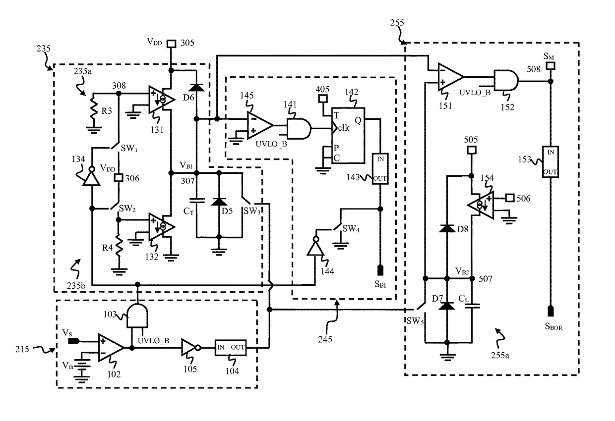
[0052]Referring to FIGS. 2, 6 and 8, the device for detecting the input voltage and discharging the residue voltage of the present invention includes a detection unit 215 further including a comparator 102 that transmits a drive signal to turn off or on the switches SW1 to SW5. A threshold voltage VTH (greater than zero) is provided to the inverting input terminal of the comparator 102, and the source of JFET 101 is connected to the non-inverting input terminal of the comparator 102. Although the output drive signal of the comparator 102 can drive the switches directly, but as an option, the drive signal together with an under voltage lockout inverted signal UVLO_B can be supplied simultaneously to two input terminal of the AND gate 103, which is also provided in the detection unit 215. The output of the AND gate 103 is connected to the input of an inverter 134 of a triangle signal generator 235, where the output terminal of the inverter 134 is connected to the control terminal of the switch SW1, while the output of the AND gate 103 is also coupled to the control terminal of the switch SW2, and the AND gate 103 is enabled such that when the under voltage lockout inverting signal UVLO_B is high level, the output of the AND gate 103 is valid, or when the inverting under voltage lockout signal UVLO_B is low level, the drive signal delivered to the switches SW1, SW2 is clamped at the low level and interrupts the charge and discharge cycles of the first capacitor CT and second capacitor CL.

Problems solved by technology

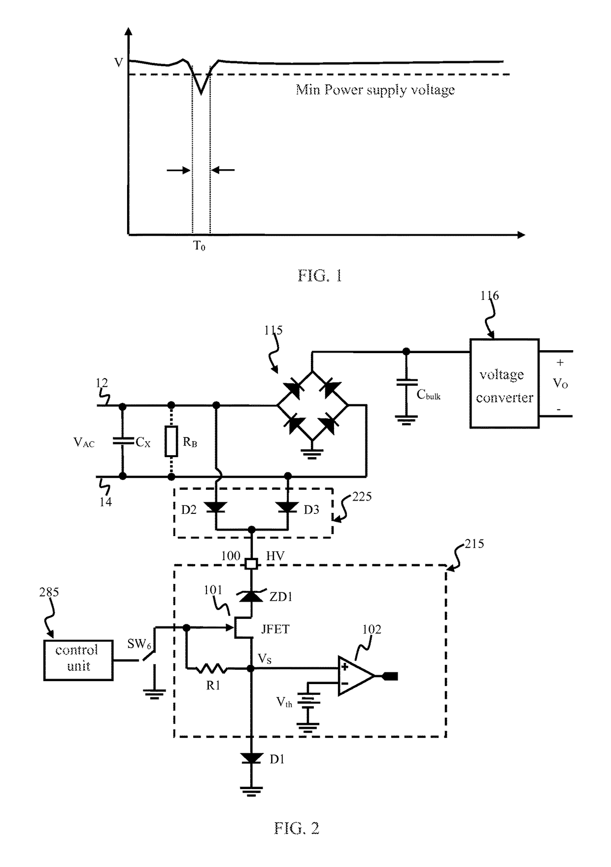
The conventional technique employed by the AC-DC conversion systems of prior art faces a problem is that the peak value or the effective value, which is also called the root mean square (RMS) value, of the AC input voltage VAC is not constant at all times. When the AC input voltage VAC from the mains electricity is in under voltage or over voltage condition, such as shown in FIG.
1 when the DC voltage V in the period T0 falls below the minimum power supply voltage, for example, usually resulting in flickering or dimming of the display, which may cause damage to the AC-DC converter.
The two resistors are connected in series between the DC output VM of the AC input voltage VAC power supply and the ground, which is well known in the art, and are turned on thus generating a current flowing through the two resistors, as a result, the resistors consume power, even though the two resistors merely serve as auxiliary detection components.
In view of this, the requirement of a device that can effectively detect changes in input voltage VAC, accurately reflects the trends of voltage VAC, but at the same time able to avoid unnecessary excessive power consumption is a big challenge.
This implementation introduces negative impact as well.
Unfortunately, if the AC power is removed at the peak of the AC voltage, the residue DC voltage equals the maximum AC voltage, which can easily cause a risk of an electric shock.
However the use of the bleeding resistor RB would result in power loss, which can be calculated by:
The power loss resulted from bleeding resistor RB is a serious matter for AC-DC converter, especially under no-load or standby condition.
Hence it is a challenge to determine the instance to remove the AC power and to discharge the residue voltage without increasing power loss.

Method used


Image

  • Methods and devices for detecting the input voltage and discharging the residuevoltage
  • Methods and devices for detecting the input voltage and discharging the residuevoltage
  • Methods and devices for detecting the input voltage and discharging the residuevoltage

Examples


Embodiment Construction

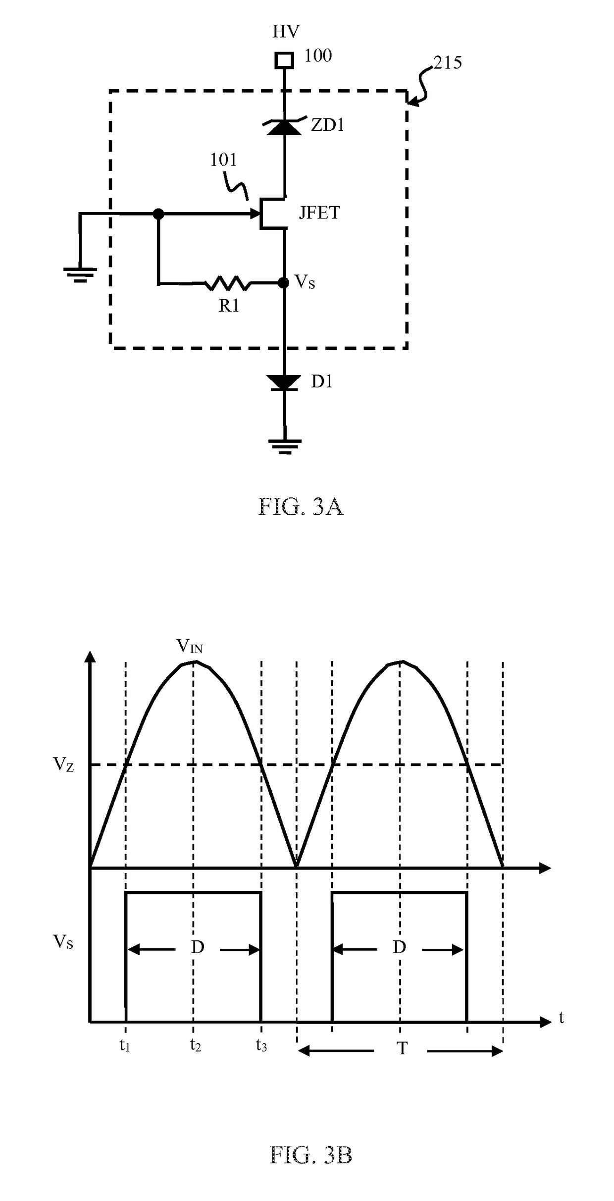
[0018]Referring to FIG. 2, a basic detection unit 215 mainly comprises a junction field effect transistor (JFET) 101 and a Zener diode ZD1, where the anode of the Zener diode ZD1 is connected to the drain of the JFET 101, and the source of JFET 101 is connected to the anode of a diode D1, while the cathode of diode D1 is connected to the ground. In addition, an electronic switch SW6, which is a main switch, is connected between the control terminal, such as the gate of JFET 101 and the ground. Switch SW6 is a three port device having a control terminal coupled to a logic control unit 285 with one end connected to the gate of JFET 101 and the other end connected directly to the ground. When the switch SW6 is on or off, the control unit 285 determines whether the gate of JFET 101 is connected to the ground potential. A resistor R1 is connected between the gate and source of JFET 101. An input DC voltage VIN is fed to the detection unit 215 at node 100 connected to the cathode of the Z...


PUM


Abstract

The present invention relates to power conversion systems, specifically, it relates to a device for detecting the DC voltage rectified from the AC power supply voltage in an AC-DC converter, primarily used to determine whether the DC input voltage is under a brown-out level and to monitor whether the AC power supply is removed and to discharge the residue DC voltage generated in a high frequency filter capacitor, which is used to filter high frequency noise signals of the AC power supply, during the removal of the AC power.

Description

PRIORITY CLAIM[0001]This application claims the priority benefit of a Chinese patent application number 201410728910.1 filed Dec. 3, 2014 by a common inventor of this Application. The entire Disclosure made in the Chinese patent application number 201410728910.1 is hereby incorporated by reference.FIELD OF PRESENT INVENTION[0002]The present invention relates to power conversion systems, specifically, it relates to a device for detecting the DC voltage rectified from the AC power supply voltage in an AC-DC converter, primarily used to determine whether the DC input voltage is under a brown-out state and to monitor whether the AC power supply is removed and to discharge the residue DC voltage generated in a high frequency filter capacitor, which is used to filter high frequency noise signals of the AC power supply, during the removal of the AC power.BACKGROUND OF RELATED ART[0003]In the conventional power conversion system, AC-DC converters are used to convert the AC input voltage VAC...

Claims


Application Information

Patent Timeline
Patent Type & Authority Patents(United States)
IPC IPC(8): G01R19/00G01R19/22H02M7/04H02M1/32
CPCG01R19/22G01R19/0007H02M1/32H02M2001/322H02M1/322
Inventor CHEN, YU-MINGLIU, CHIH-YUANHUANG, PEI-LUN
Owner ALPHA AND OMEGA SEMICONDUCTOR (CAYMAN) LIMITED
Learn More