Storage scheme for built-in ECC operations

a storage scheme and built-in ecc technology, applied in the field of integrated circuit memory devices, can solve the problems of reducing the read throughput of the memory device, and the data from the next data page cannot be moved to the cach

Active Publication Date: 2017-06-27
MACRONIX INT CO LTD
View PDF14 Cites 18 Cited by
  • Summary
  • Abstract
  • Description
  • Claims
  • Application Information

AI Technical Summary

Benefits of technology

[0015]Other aspects and advantages of the present invention can be seen on review of the drawings, the detailed description and the claims, which follow.

Problems solved by technology

However, data from a next data page cannot be moved to the cache until after the corrected data in the cache has been moved from the cache to the data path.
This results in a lower read throughput for the memory device.

Method used


Image

  • Storage scheme for built-in ECC operations
  • Storage scheme for built-in ECC operations
  • Storage scheme for built-in ECC operations

Examples


first embodiment

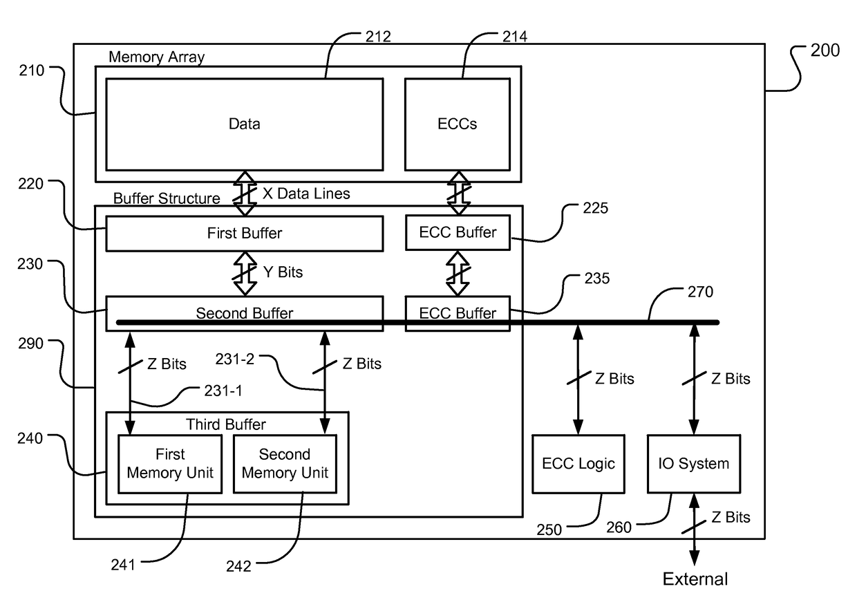
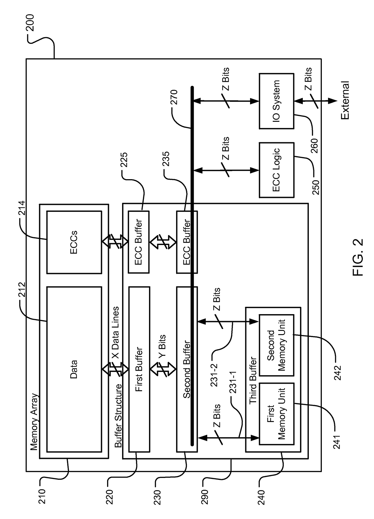
[0039]FIG. 2 is a simplified block diagram of a memory device 200 using built-in error correcting ECC logic. The memory device 200 includes a memory array 210 storing data 212 and error correcting codes ECCs 214 corresponding to the data, and a multi-level buffer structure 290 between the memory array and an input / output data path 270. The memory array includes a plurality of data lines 211 for page mode operations. The buffer structure includes a first buffer 220 having storage cells connected to respective data lines in the plurality of data lines for a page of data, a second buffer 230 coupled to the storage cells in the first buffer for storing at least one page of data, and a third buffer 240 coupled to the second buffer and to the input / output data path. The device includes logic coupled to the multi-level buffer to perform a logical process over pages of data during movement between the memory array and the input / output path through the multi-level buffer for at least one of ...

second embodiment

[0078]FIG. 7 is a simplified block diagram of a memory device 700 using built-in error correcting ECC logic. The device 700 includes a memory array 710 storing data 712 and error correcting codes ECCs 714 corresponding to the data, an input / output data path, and a multi-level buffer structure 790 between the memory array and the input / output data path. The memory array includes a plurality of data lines 711 for page mode operations. The multi-level buffer structure 290 includes a first buffer 720 having storage cells connected to respective data lines in the plurality of data lines for a page of data, a second buffer 730 coupled to the storage cells in the first buffer for storing at least one page of data, and a third buffer 740 coupled to the second buffer and to the input / output data path. The device 700 includes logic coupled to the multi-level buffer to perform a logical process over pages of data during movement between the memory array and the input / output path through the mu...


PUM

PropertyMeasurementUnit
timeaaaaaaaaaa
timeaaaaaaaaaa
timeaaaaaaaaaa

Abstract

A device includes a memory array storing data and error correcting codes ECCs corresponding to the data, and a multi-level buffer structure between the memory array and an input / output data path. The memory array includes a plurality of data lines for page mode operations. The buffer structure includes a first buffer having storage cells connected to respective data lines in the plurality of data lines for a page of data, a second buffer coupled to the storage cells in the first buffer for storing at least one page of data, and a third buffer coupled to the second buffer and to the input / output data path. The device includes logic coupled to the multi-level buffer to perform a logical process over pages of data during movement between the memory array and the input / output path through the multi-level buffer for at least one of page read and page write operations.

Description

CROSS-REFERENCE TO RELATED APPLICATIONS[0001]This application claims the benefit of U.S. Provisional Patent Application No. 61 / 775,699, filed 11 Mar. 2013.BACKGROUND OF THE INVENTION[0002]Field of the Invention[0003]The present invention relates to integrated circuit memory devices, and to circuitry using error correcting codes ECCs.[0004]Description of Related Art[0005]High density memory devices are being designed that include arrays of flash memory cells, or other types of memory cells. In one example, a memory device includes a memory array storing data pages and error correcting codes ECCs for corresponding data pages. The device includes ECC logic to detect and correct errors in the corresponding data pages using the ECCs. The device includes a page buffer coupled to the memory array, to the ECC logic, and to a data path. The page buffer includes sense amplifiers for read operations, a program buffer for write operations, and a cache for read and write operations on data in a ...

Claims


Application Information

Patent Timeline
Patent Type & Authority Patents(United States)
IPC IPC(8): G11C29/00G06F11/10G11B20/18G11C7/10
CPCG06F11/1044G06F11/1008G06F11/1068G11B20/1833G11C7/1006
Inventor LIU, YI-CHINGLO, CHIHUNG, SHUO-NANHUNG, CHUN-HSIUNG
Owner MACRONIX INT CO LTD
Why Eureka
Try Eureka