Organic light-emitting display device

a display device and organic technology, applied in static indicating devices, organic semiconductor devices, instruments, etc., can solve the problems of unnecessarily emitting light, driving pixels, and adjacent pixels, and lowering the display quality of organic light-emitting display devices. , the effect of reducing the emission of undesired pixels due to the leakage curren

Active Publication Date: 2017-08-01
LG DISPLAY CO LTD
View PDF5 Cites 0 Cited by
  • Summary
  • Abstract
  • Description
  • Claims
  • Application Information

AI Technical Summary

Benefits of technology

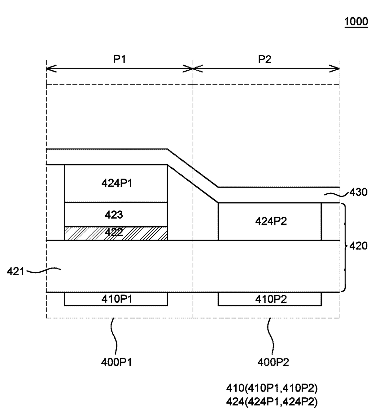
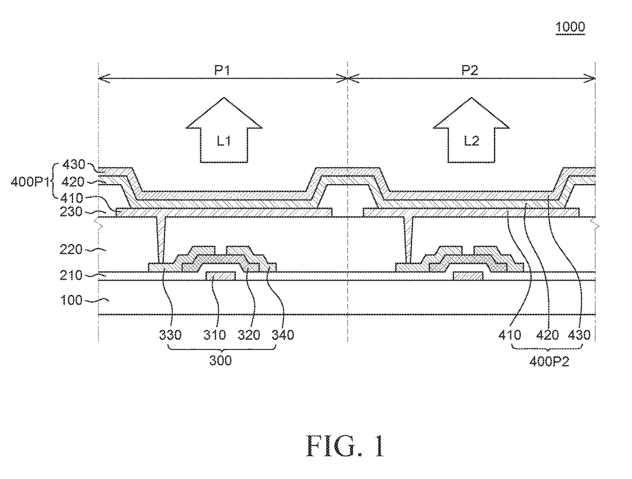
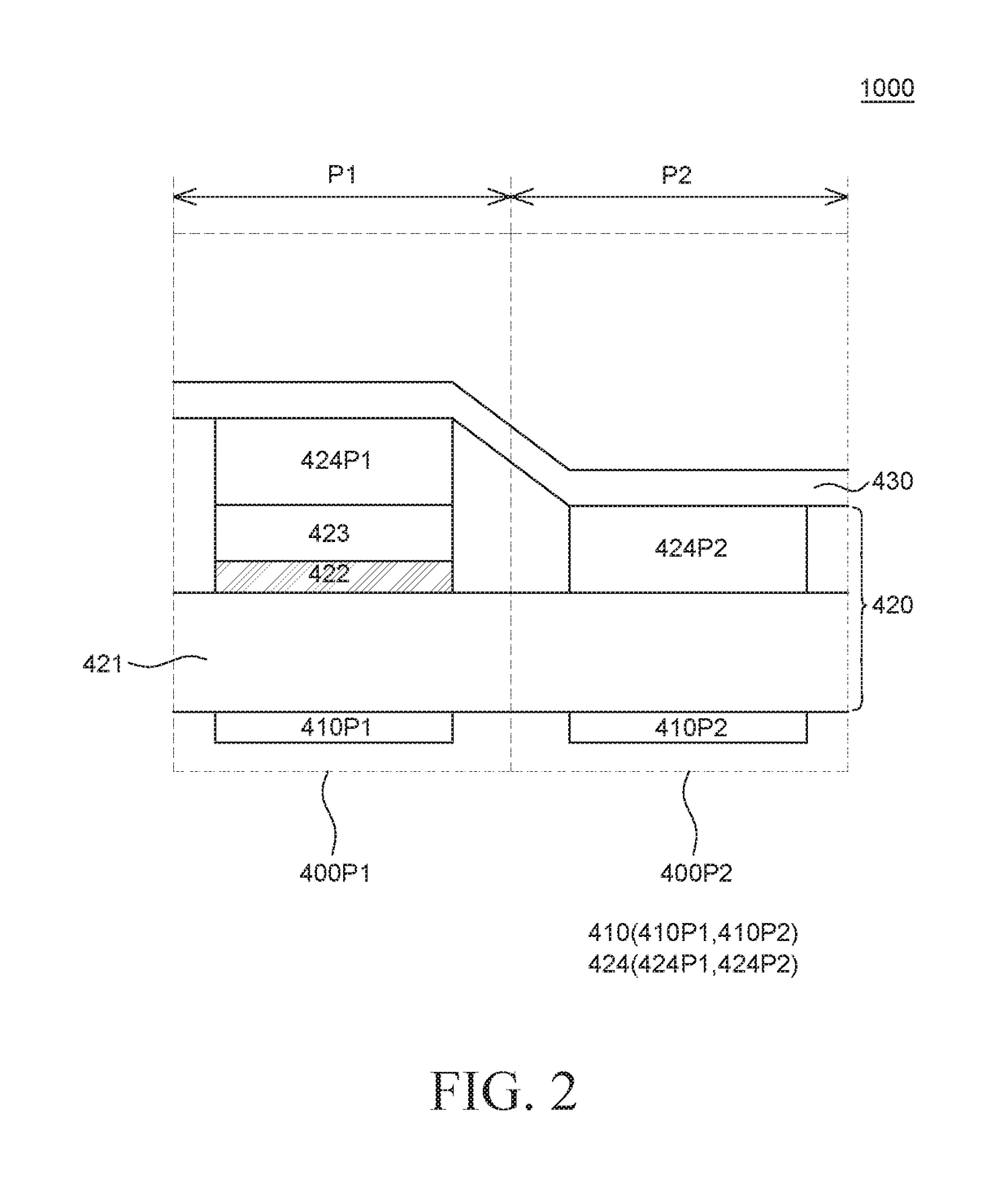
[0009]Organic layers, such as an injecting layer or a transporting layer, which improve characteristics of the light-emitting elements such as a driving voltage or light emission efficiency may be further disposed between two electrodes. Further, each pixel may have different lamination structures in consideration of a characteristic of the light-emitting layers which are patterned for every pixel, in consideration of wavelengths, materials, and the like.
[0027]A thickness of the functional layer is a thickness obtained by considering a micro-cavity distance between two electrodes, so that an optical efficiency and a lifespan of the organic light-emitting display device is improved.

Problems solved by technology

However, if an organic layer is formed to have a common structure and shared by the plurality of pixels, when the organic light-emitting display device is driven, some currents are leaked through the organic layer having a common structure.
Therefore, not only the driving pixel, but also adjacent pixels unnecessarily emit light.
Therefore, unexpected pixels unnecessarily emit light to cause color mixture between pixels, which results in lowered display quality of the organic light-emitting display device.
Further, the current flowing into the organic layer having a common structure is easily leaked to the pixel having a lower turn-on voltage which is considered to have a lower barrier through which the current flows.
Therefore, the color mixture due to the leaked current may be more seriously noticed at a low gray scale.

Method used


Image

  • Organic light-emitting display device
  • Organic light-emitting display device
  • Organic light-emitting display device

Examples


Embodiment Construction

[0037]Advantages and features of the present disclosure, and methods for accomplishing the same will be more clearly understood from exemplary embodiments described below with reference to the accompanying drawings. However, the present disclosure is not limited to exemplary embodiment disclosed herein but will be implemented in various forms. The exemplary embodiments are provided by way of example only so that a person of ordinary skilled in the art can fully understand the disclosures of the present disclosure and the scope of the present disclosure. Therefore, the present disclosure will be defined only by the scope of the appended claims.

[0038]The shapes, sizes, ratios, angles, numbers, and the like illustrated in the accompanying drawings for describing the exemplary embodiments of the present disclosure are merely examples, and the present disclosure is not limited thereto. Like reference numerals indicate like elements throughout the specification. Further, in the following ...


PUM


Abstract

Provided is a display device, including two light-emitting elements having different turn-on voltages. Each of the light-emitting elements includes a patterned electrode, a common layer, a patterned light-emitting layer, and a common electrode. The light-emitting element with the lower turn-on voltage among the two light-emitting elements includes a functional layer which suppresses a hole from being leaked from the light-emitting layer with the higher turn-on voltage through the common layer when the light-emitting element with the higher turn-on voltage among the two light-emitting elements is driven at a low gray scale to move into the patterned light-emitting layer of the light-emitting element with the lower turn-on voltage. Therefore, the light emission of an undesired pixel due to the leakage current is reduced, thereby improving the display quality.

Description

CROSS-REFERENCE TO RELATED APPLICATIONS[0001]This application claims the priority of Korean Patent Application No. 10-2015-0112391 filed on Aug. 10, 2015, in the Korean Intellectual Property Office, the disclosure of which is incorporated herein by reference.BACKGROUND OF THE INVENTION[0002]Field of the Invention[0003]The present disclosure relates to an organic light-emitting display device, and more particularly, to an organic light-emitting display device which suppresses a current leaked through a common layer shared by a plurality of light-emitting elements, from flowing into an adjacent light-emitting element, to improve a display quality.[0004]Description of the Related Art[0005]An organic light-emitting display device (OLED device) is the next-generation display apparatus having a self-luminance characteristic. Unlike a liquid crystal display device, the organic light-emitting display device does not need a separate light source. Thus, the organic light emitting device may b...

Claims


Application Information

Patent Timeline
Patent Type & Authority Patents(United States)
IPC IPC(8): H01L29/08G09G3/3258G09G3/3266H01L27/32H01L51/50H01L51/52H01L27/15H01L27/14G09G3/20H01L29/06
CPCH01L51/5265G09G3/2074G09G3/3258G09G3/3266H01L27/3211H01L27/3244H01L51/5004H01L51/5056H01L51/5206H01L51/5221G09G2300/0452G09G2300/0819G09G2320/0242H01L2251/552H01L2251/558H10K59/1213H10K50/15H10K59/35H10K59/12H10K50/11H10K2101/40H10K50/156H10K50/852H10K2101/30H10K50/81H10K50/82H10K2102/351
Inventor LEE, SOHEE
Owner LG DISPLAY CO LTD
Why Eureka
Try Eureka