Electronic component mounting device and semiconductor device including the same

a technology for mounting devices and electronic components, applied in the direction of final product manufacturing, semiconductor/solid-state device details, sustainable manufacturing/processing, etc., can solve the problems of adverse effects on melf electronic components in some cases, and achieve the effect of reducing thermal stress and suppressing the positional displacement of melf electronic components

Active Publication Date: 2017-08-01
MITSUBISHI ELECTRIC CORP
View PDF29 Cites 0 Cited by
  • Summary
  • Abstract
  • Description
  • Claims
  • Application Information

AI Technical Summary

Benefits of technology

[0007]The present invention has been made in view of the above-mentioned problems, and an object thereof is to provide the technique capable of suppressing the positional displacement of the MELF electronic component and reducing the thermal stress applied to the MELF electronic component.
[0009]The MELF electronic component is fitted into the first receiving portion or the second receiving portion, to thereby suppress the positional displacement between the insulating substrate and the MELF electronic component. The thermal stress applied to the MELF electronic component from the insulating substrate can also be reduced.

Problems solved by technology

Thus, while the thermal stress of the mounting substrate remains relatively high, the thermal stress is applied to the MELF electronic component, resulting in adverse effects on the MELF electronic component in some cases.

Method used


Image

  • Electronic component mounting device and semiconductor device including the same
  • Electronic component mounting device and semiconductor device including the same
  • Electronic component mounting device and semiconductor device including the same

Examples


first preferred embodiment

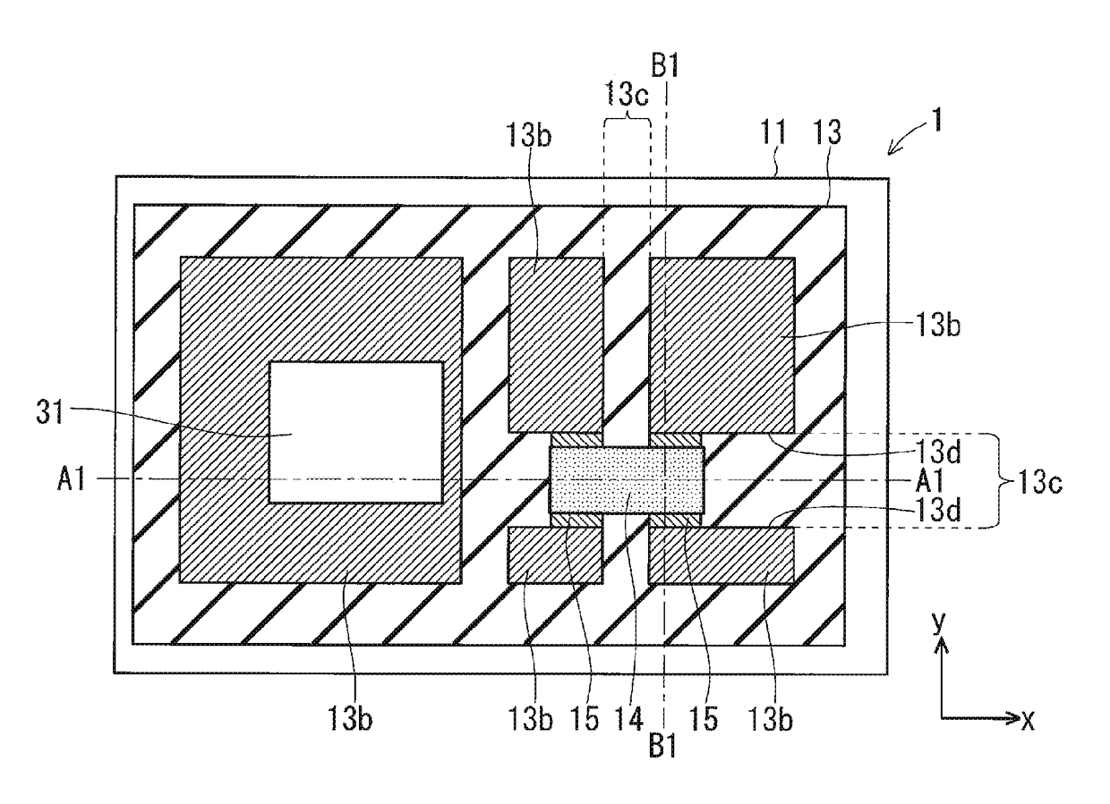
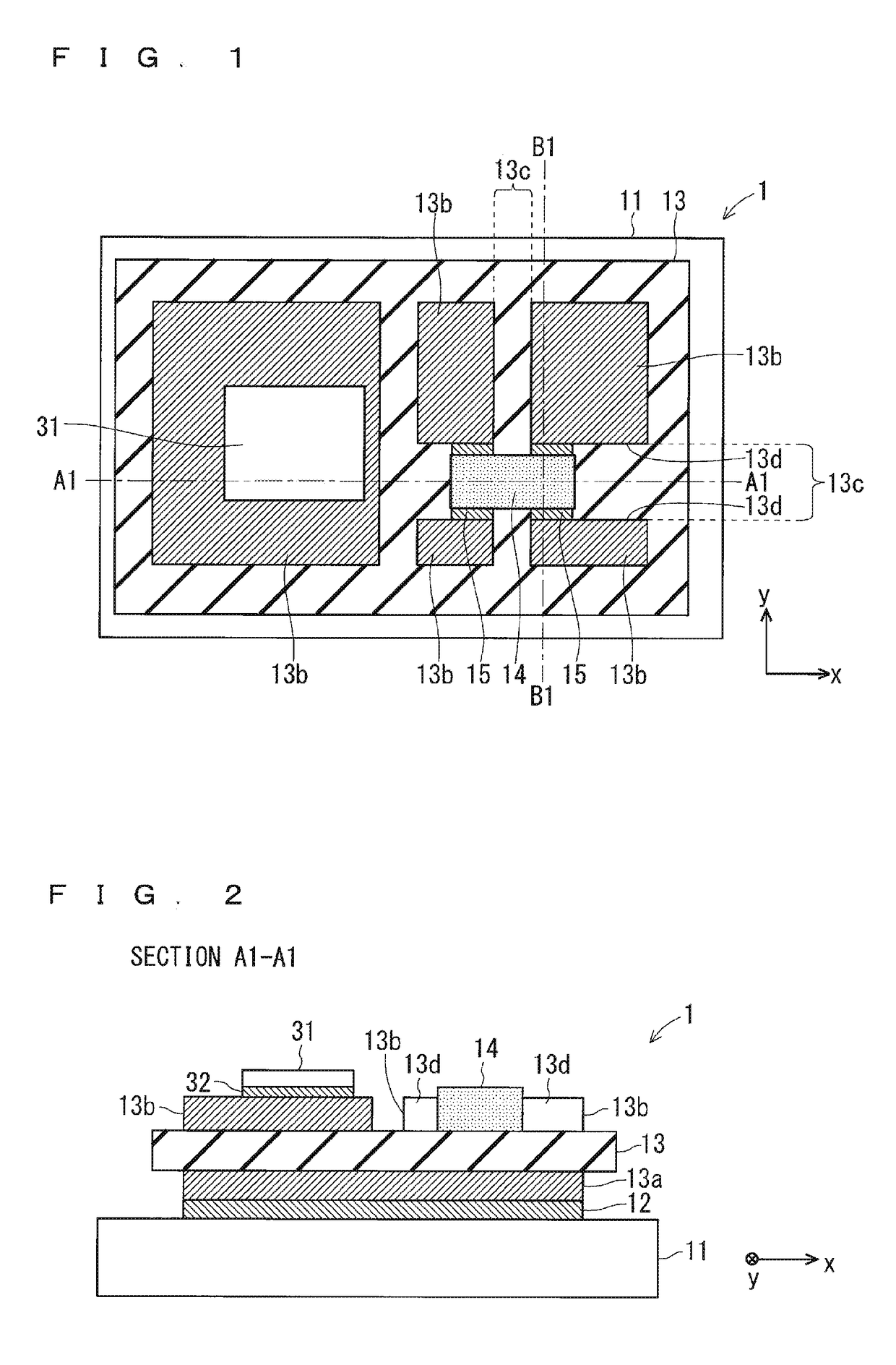
[0026]FIG. 1 is a top view showing a configuration of a semiconductor device according to a first preferred embodiment of the present invention, FIG. 2 is a cross-sectional view showing the configuration taken along an A1-A1 line of FIG. 1, and FIG. 3 is a cross-sectional view showing the configuration taken along a B1-B1 line of FIG. 1.

[0027]As shown in FIGS. 1 to 3, the semiconductor device according to the first preferred embodiment includes an electronic component mounting device 1, a power semiconductor element 31, and a solder 32. The electronic component mounting device 1 includes a base plate 11, a solder 12, an insulating substrate 13, a MELF electronic component 14, and conductive members 15.

[0028]A back surface metal pattern 13a bonded to the base plate 11 with the solder 12 is formed on a back surface (lower surface in FIGS. 2 and 3) of the insulating substrate 13. Meanwhile, metal patterns 13b are formed on a front surface (upper surface in FIGS. 2 and 3) of the insulat...

second preferred embodiment

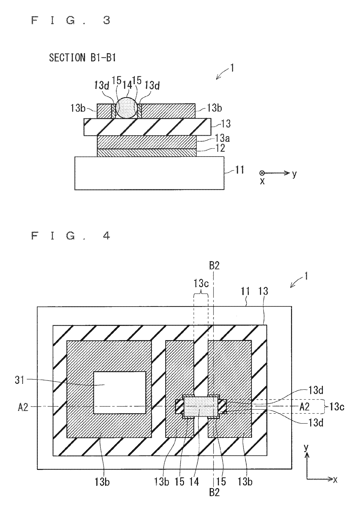
[0037]FIG. 4 is a top view showing a configuration of a semiconductor device according to a second preferred embodiment of the present invention, FIG. 5 is a cross-sectional view showing the configuration taken along an A2-A2 line of FIG. 4, and FIG. 6 is a cross-sectional view showing the configuration taken along a B2-B2 line of FIG. 4. In the semiconductor device according to the second preferred embodiment, the same or similar components as those described above are denoted by the same references while the differences are mainly described below.

[0038]As shown in FIGS. 4 to 6, in the second preferred embodiment similar to the first preferred embodiment, the metal patterns 13b and the insulating substrate 13 exposed from the lacking portion of the metal patterns 13b form the first receiving portion 13c. However, in the second preferred embodiment unlike the first preferred embodiment, the lacking portion of the metal patterns 13b extends from −y side end to +y side end of the meta...

third preferred embodiment

[0042]FIG. 7 is a top view showing a configuration of a semiconductor device according to a third preferred embodiment of the present invention, FIG. 8 is a cross-sectional view showing the configuration taken along an A3-A3 line of FIG. 7, and FIG. 9 is a cross-sectional view showing the configuration taken along a B3-B3 line of FIG. 7. In the semiconductor device according to the third preferred embodiment, the same or similar components as those described above are denoted by the same references while the differences are mainly described below.

[0043]As shown in FIGS. 7 to 9, in the third preferred embodiment similar to the first preferred embodiment, the metal patterns 13b and the insulating substrate 13 exposed from the lacking portion of the metal patterns 13b form the first receiving portion 13c. The side portions 13d facing each other of the metal patterns 13b cut in a cross shape by the lacking portion to be divided into four in plan view and the insulating substrate 13 expo...


PUM


Abstract

An electronic component mounting device includes an insulating substrate having a metal pattern formed thereon and a MELF electronic component. The MELF electronic component is fitted into a first receiving portion configured with the metal pattern and the insulating substrate exposed from a lacking portion of the metal pattern. The electronic component mounting device further includes a conductive member formed between the MELF electronic component and the metal pattern, and the conductive member is not formed between the MELF electronic component and the insulating substrate.

Description

BACKGROUND OF THE INVENTION[0001]Field of the Invention[0002]The present invention relates to an electronic component mounting device having a MELF electronic component mounted on an insulating substrate and to a semiconductor device including the electronic component mounting device.[0003]Description of the Background Art[0004]The variety of techniques for suppressing a positional displacement upon mounting of a MELF electronic component on a mounting substrate has been developed. For example, the technique disclosed in Japanese Patent Application Laid-Open No. 2006-32511 forms the U-shaped (square U-shaped) conductive electrode having the inner dimensions greater than the diameter of the MELF electronic component, whereby the above-mentioned positional displacement can be suppressed.[0005]In general, activating an electronic component, a semiconductor element, or the like mounted on a mounting substrate generates heat which will be conducted to the mounting substrate, and then the...

Claims


Application Information

Patent Timeline
Patent Type & Authority Patents(United States)
IPC IPC(8): H05K1/18H05K1/11H05K3/34H01L23/15H05K7/12H05K7/00H01L23/373H01L23/13H01L23/498
CPCH05K1/183H01L23/15H01L23/49838H05K1/11H05K1/111H05K3/3442H01L23/13H01L23/3735H01L23/49827H01L23/49844H01L2224/32225H01L2924/19105H05K1/186H05K1/188H05K2201/09072H05K2201/09745H05K2201/10H05K2201/1059H05K2201/10174H05K2201/10636H05K2201/10651H05K2201/10674H05K2201/10689Y02P70/611Y02P70/613H05K3/38Y02P70/50
Inventor OBARA, TAICHIYONEYAMA, REIOTSUKI, TAKAMISHITAMA, EIJU
Owner MITSUBISHI ELECTRIC CORP
Why Eureka
Try Eureka