
Shift register with multiple discharge voltages

a technology of shift register and discharge voltage, which is applied in the field of shift register, can solve the problems of affecting the operation of the display apparatus equipped with the shift register, and affecting the operation of the display apparatus. , to achieve the effect of reducing leakage current, reducing leakage current, and increasing the margin between scan pulses

Active Publication Date: 2017-08-08
LG DISPLAY CO LTD
View PDF13 Cites 4 Cited by
  • Summary
  • Abstract
  • Description
  • Claims
  • Application Information

AI Technical Summary

Benefits of technology

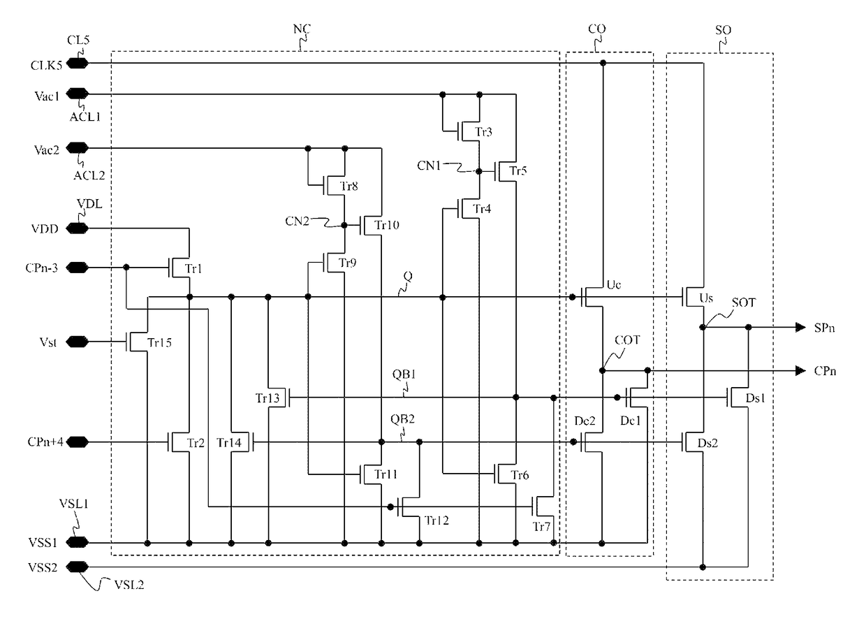
This design reduces leakage current, shortens the falling edge time of scan pulses, and minimizes the size of the shift register and display apparatus, enhancing image quality and reducing bezel size without increasing the size of the output switching elements.

Problems solved by technology

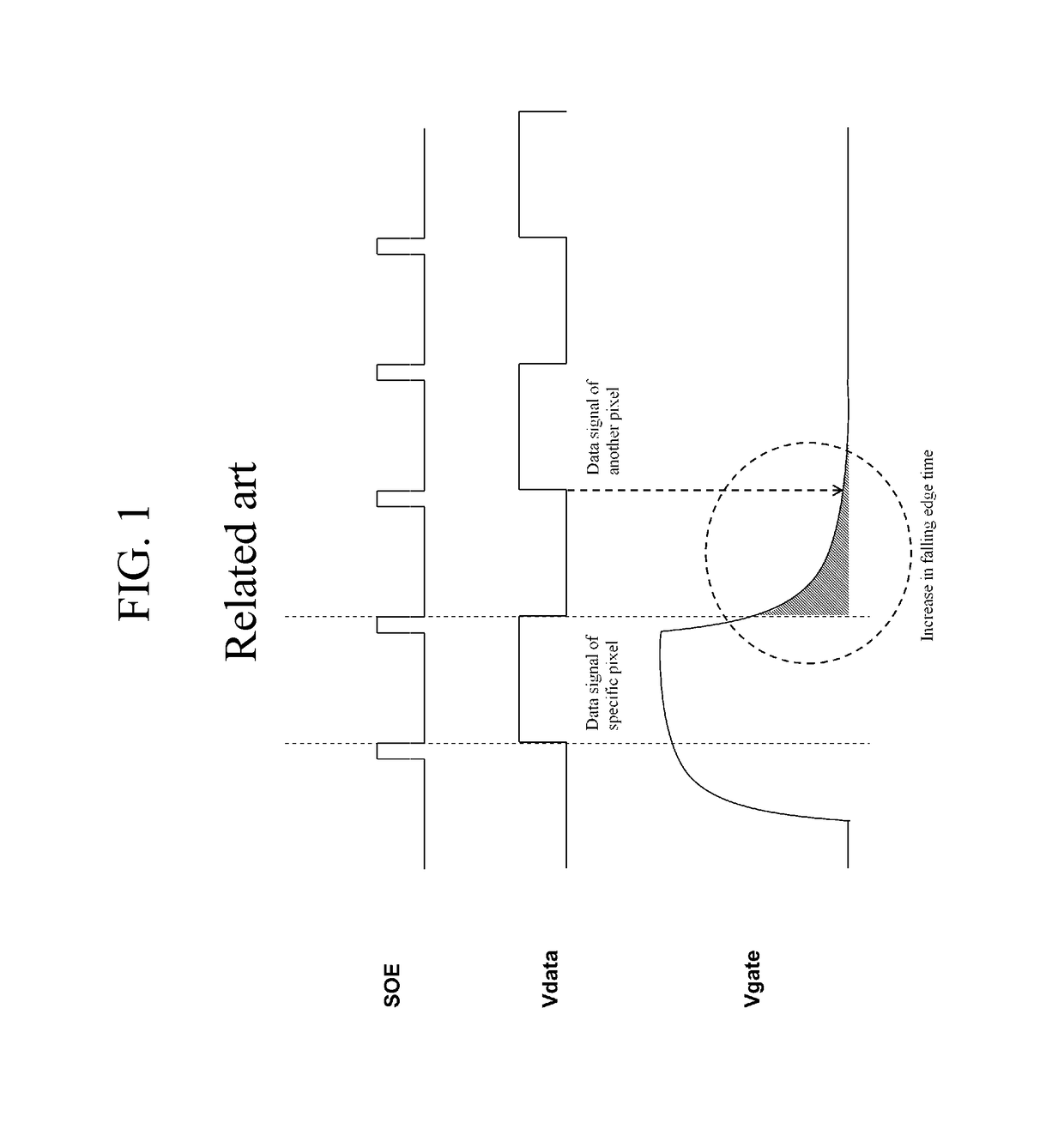
When such an output switching element is degraded due to prolonged driving thereof, the wavelength of a scan pulse generated from the output switching element may become distorted.
As a result, the pixel may display an erroneous image and degradation of picture quality may occur.
As such, there may be another problem in that the size of the display apparatus equipped with the shift register is increased.

Method used


Image

  • Shift register with multiple discharge voltages
  • Shift register with multiple discharge voltages
  • Shift register with multiple discharge voltages

Examples


Embodiment Construction

[0042]Reference will now be made in detail to the preferred embodiments of the present invention, examples of which are illustrated in the accompanying drawings.

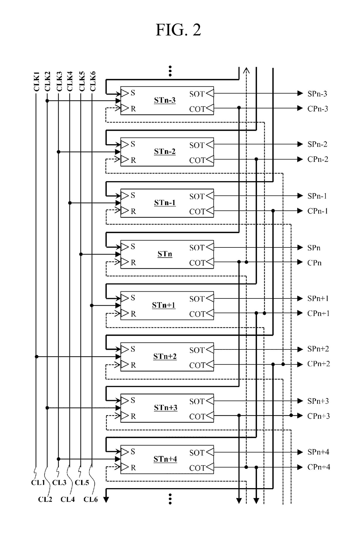
[0043]FIG. 2 is a diagram illustrating a shift register according to an embodiment. FIG. 3 is a timing diagram of various signals supplied to or output from stages included in the shift register of FIG. 2.

[0044]As illustrated in FIG. 2, the shift register includes a plurality of stages. For instance, FIG. 2 shows stages STn−3 to STn+4.

[0045]The stages output pulses in a sequential manner. That is, the stages . . . , STn−3 to STn+4, . . . output pulses in a sequentially manner in order from the first stage to the last stage (hereinafter, referred to an “m-th stage”), respectively. In detail, each of the stages . . . , STn−3 to STn+4, . . . includes a scan output terminal SOT and a carry output terminal COT. Each of the stages . . . , STn−3 to STn+4, . . . outputs a corresponding one of scan pulses SP1 to SPn once in one frame...


PUM


Abstract

A shift register for reducing size of a display apparatus through a reduction in falling edge time of a scan pulse. The shift register includes stages for sequentially outputting carry pulses and scan pulses. Each stage includes a carry output unit for generating a carry pulse, based on a first discharge voltage and a clock pulse having a low-level voltage with a level substantially equal to the first discharge voltage, and supplying the carry pulse to at least one of an upstream stage and a downstream stage, a scan output unit for generating a scan pulse, based on a second discharge voltage having a higher voltage value than the first discharge voltage and the clock pulse, and supplying the scan pulse to a corresponding gate line, and a node controller for controlling voltages at nodes connected to the carry output unit and the scan output unit.

Description

CROSS REFERENCE TO RELATED APPLICATIONS[0001]This application claims the benefit of the Korean Patent Application No. 10-2013-0074206, filed on Jun. 27, 2013 which is hereby incorporated by reference as if fully set forth herein.BACKGROUND[0002]Field of the Invention[0003]The present invention relates to a shift register and, more particularly, to a shift register capable of reducing size of a display apparatus through reduction in the falling edge time of a scan pulse.[0004]Discussion of the Related Art[0005]In general, a liquid crystal display (LCD) device is adapted to display an image by adjusting light transmittance of a liquid crystal using an electric field. To this end, the LCD device includes a liquid crystal panel having pixel areas arranged in matrix form, and a driving circuit for driving the liquid crystal panel.[0006]In the liquid crystal panel, a plurality of gate lines and a plurality of data lines are arranged to cross each other, and the pixel areas are defined res...

Claims


Application Information

Patent Timeline
Patent Type & Authority Patents(United States)
IPC IPC(8): G09G3/36G11C19/28
CPCG09G3/3677G11C19/28G09G2310/0286G09G2310/08G09G2320/0209G09G2320/0223G09G3/36G11C19/00
Inventor JO, SUNG-HAK
Owner LG DISPLAY CO LTD
Learn More